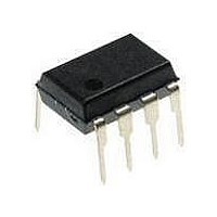
TISPPBL1P-S Bourns Inc., TISPPBL1P-S Datasheet - Page 2

TISPPBL1P-S
Manufacturer Part Number
TISPPBL1P-S
Description
Sidacs
Manufacturer
Bourns Inc.
Datasheet
1.TISPPBL3-S.pdf
(18 pages)
Specifications of TISPPBL1P-S
Mounting Style
Through Hole
Package / Case
PDIP-8
Lead Free Status / RoHS Status
Lead free / RoHS Compliant
TISPPBL1D, TISPPBL1P, TISPPBL2D, TISPPBL2P
DUAL FORWARD-CONDUCTING P-GATE THYRISTORS
FOR ERICSSON COMPONENTS SLICS
description
absolute maximum ratings, -40 °C
NOTES: 1. Initially the protector must be in thermal equilibrium with -40 °C
Repetitive peak off-state voltage, I
Repetitive peak gate-cathode voltage, V
Non-repetitive peak on-state pulse current (see Notes 1 and 2)
Non-repetitive peak on-state current, 50/60 Hz (see Notes 1 and 2)
Non-repetitive peak gate current, 1/2 µs pulse, cathodes commoned (see Note 1)
Operating free-air temperature range
Junction temperature
Storage temperature range
2
The protector gate is connected to this negative supply. This references the protection (clipping) voltage to the
negative supply voltage. As the protection voltage will track the negative supply voltage the overvoltage stress
on the SLIC is minimised. The TISPPBLx buffered gate design reduces the loading on the SLIC supply during
overvoltages caused by power cross and induction.
Positive overvoltages are clipped to ground by diode forward conduction. Negative overvoltages are initially
clipped close to the SLIC negative supply rail value. If sufficient current is available from the overvoltage, then
the protector will crowbar into a low voltage ground referenced on-state condition. As the overvoltage
subsides the high holding current of the crowbar prevents d.c. latchup. The difference between the TISPPBL1
and TISPPBL2 is the minimum value of holding current. The 105 mA TISPPBL1 can delatch SLIC
programmed line currents up to 55 mA and the 150 mA TISPPBL2 can delatch all programmed line current
values.
These monolithic protection devices are fabricated in ion-implanted planar vertical power structures for high
reliability and in normal system operation they are virtually transparent. The TISPPBLx is available in 8-pin
plastic small-outline surface mount package and 8-pin plastic dual-in-line package.
The TISPPBL1 and TISPPBL2 are dual forward-conducting buffered p-gate overvoltage protectors. They are
designed to protect the Ericsson Components SLICs (Subscriber Line Interface Circuits) against overvoltages
on the telephone line caused by lightning, a.c. power contact and induction. The TISPPBLx limits voltages
that exceed the SLIC supply rail levels.
The SLIC line driver section is typically powered by a negative voltage, V
10/1000 µs (Bellcore GR-1089-CORE, Issue 2, December 1997, Section 4)
0.2/310 µs (I3124, open-circuit voltage wave shape 0.5/700 µs)
5/310 µs (ITU-T K20 & K21, open-circuit voltage wave shape 10/700 µs)
1/20 µs (ITU-T K22, open-circuit voltage wave shape 1.2/50 µs)
2/10 µs (Bellcore GR-1089-CORE, Issue 2, December 1997, Section 4)
100 ms
1 s
5 s
300 s
900 s
2. These non-repetitive rated currents are peak values for either polarity. The rated current values may be applied either to the Ring to
its initial conditions.
Ground or to the Tip to Ground terminal pairs. Additionally, both terminal pairs may have their rated current values applied
simultaneously (in this case the Ground terminal current will be twice the rated current value of an individual terminal pair). Above
85 °C, derate linearly to zero at 150 °C lead temperature.
G
= 0
KA
= 0
RATING
T
A
85 °C (unless otherwise noted)
T
J
P R O D U C T
85 °C. The surge may be repeated after the device returns to
Specifications are subject to change without notice.
Bat
AUGUST 1997 - REVISED AUGUST 2002
SYMBOL
, in the region of -10 V to -85 V.
V
V
I
I
GKRM
I
T
GSM
TSM
TSP
DRM
T
T
stg
I N F O R M A T I O N
A
J
-40 to +150
-65 to +150
-40 to +85
VALUE
-100
0.95
0.93
100
100
-90
4.5
2.4
30
40
40
11
40
UNIT
°C
°C
°C
V
V
A
A
A


