1PS10SB82 T/R NXP Semiconductors, 1PS10SB82 T/R Datasheet
1PS10SB82 T/R
Specifications of 1PS10SB82 T/R


Related parts for 1PS10SB82 T/R


1PS10SB82 T/R Summary of contents
Page 1
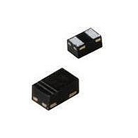
DATA SHEET M3D891 BOTTOM VIEW 1PS10SB82 Schottky barrier diode Product data sheet DISCRETE SEMICONDUCTORS 2003 Aug 20 ...
Page 2
... NXP Semiconductors Schottky barrier diode FEATURES • Low forward voltage • Low diode capacitance • Leadless ultra small plastic package (1.0 mm × 0.6 mm × 0.5 mm) • Boardspace 1. (approx. 10% of SOT23) • Power dissipation comparable to SOT23. APPLICATIONS • UHF mixers • Sampling circuits • ...
Page 3
... NXP Semiconductors Schottky barrier diode ELECTRICAL CHARACTERISTICS = 25 °C unless otherwise specified. T amb SYMBOL PARAMETER V forward voltage F r differential diode forward resistance D I continuous reverse current R C diode capacitance d Note = 300 μs; δ = 0.02. 1. Pulse test THERMAL CHARACTERISTICS SYMBOL PARAMETER R thermal resistance from junction to ambient ...
Page 4
... NXP Semiconductors Schottky barrier diode GRAPHICAL DATA 3 10 handbook, halfpage I F (mA) ( (1) (2) ( 0.4 0.8 = 125 °C. (1) T amb = 85 °C. (2) T amb = 25 °C. (3) T amb Fig.2 Forward current as a function of forward voltage; typical values. 1.2 handbook, halfpage C d (pF) 1 0.8 0.6 0.4 ...
Page 5
... NXP Semiconductors Schottky barrier diode PACKAGE OUTLINE Leadless ultra small plastic package; 2 terminals; body 1.0 x 0 (2) DIMENSIONS (mm are the original dimensions) A (1) 1 UNIT max. 0.50 0.55 0.62 mm 0.03 0.46 0.47 0.55 Notes 1. Including plating thickness 2. The marking bar indicates the cathode ...
Page 6
... NXP Semiconductors. In case of any inconsistency or conflict between information in this document and such terms and conditions, the latter will prevail. ...
Page 7
... NXP Semiconductors Customer notification This data sheet was changed to reflect the new company name NXP Semiconductors. No changes were made to the content, except for the legal definitions and disclaimers. Contact information For additional information please visit: http://www.nxp.com For sales offices addresses send e-mail to: salesaddresses@nxp.com © ...