ADNB-6002-EV Avago Technologies US Inc., ADNB-6002-EV Datasheet - Page 18
ADNB-6002-EV
Manufacturer Part Number
ADNB-6002-EV
Description
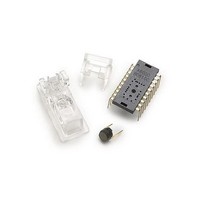
OPT SENS BUNDLE W/A-6000 TL CLIP
Manufacturer
Avago Technologies US Inc.
Specifications of ADNB-6002-EV
Description/function
Laser Mouse Bundle
Interface Type
SPI
Product
Display Modules
Touch Panel
No Touch Panel
For Use With/related Products
ADNS-6000
Lead Free Status / RoHS Status
Lead free / RoHS Compliant
Lead Free Status / RoHS Status
Lead free / RoHS Compliant, Lead free / RoHS Compliant


Motion Read
Reading the Motion_Burst register activates this mode.
The ADNS-6000 will respond with the contents of
the Motion, Delta_X, Delta_Y, SQUAL, Shutter_Upper,
Shutter_Lower, and Maximum_Pixel registers in that
order. After sending the register address, the micro-
controller must wait t
data. All 64 data bits can be read with no delay between
bytes by driving SCLK at the normal rate. The data are
latched into the output buffer after the last address bit
is received. After the burst transmission is complete, the
micro-controller must raise the NCS line for at least t
to terminate burst mode. The serial port is not available
for use until it is reset with NCS, even for a second burst
transmission.
PROM Download
This function is used to load the Avago Technologies-
supplied firmware file contents into the ADNS-6000. The
firmware file is an ASCII text file with each 2-character
byte on a single line.
The following steps activate this mode:
1. Perform hardware reset by toggling the RESET pin
2. Write 0x1D to register 0x14 (SROM_Enable register)
3. Wait at least 1 frame period
4. Write 0x18 to register 0x14 (SROM_Enable register)
5. Begin burst mode write of data file to register 0x60
Figure 23. Motion burst timing.
SCLK
Figure 24. PROM Download Burst Mode
18
SCLK
MOSI
NCS
(SROM_Load register)
SROM_Enable reg write
Motion_Burst Register Address
t
NCS-SCLK
>120ns
≥
SRAD-MOT
1 frame
period
First Read Operation
SROM_Enable reg write
address
and then begin reading
Read First Byte
≥ t
key data
SRAD-MOT
75 µs
≥ 40 µ s
BEXIT
SROM_Load reg write
Read Second Byte
address
After the first data byte is complete, the PROM or micro-
controller must write subsequent bytes by presenting
the data on the MOSI line and driving SCLK at the normal
rate. A delay of at least t
bytes as shown. After the download is complete, the
micro-controller must raise the NCS line for at least t
to terminate burst mode. The serial port is not available
for use until it is reset with NCS, even for a second burst
transmission.
register to verify that the download was successful. In
addition, a self-test may be executed, which performs a
CRC on the SROM contents and reports the results in a
register. The test is initiated by writing a particular value
to the SROM_Enable register; the result is placed in the
Data_Out register. See those register descriptions for
more details.
Avago Technologies provides the data file for download;
the file size is 1986 data bytes. The chip will ignore any
additional bytes written to the SROM_Load register after
the SROM file.
Avago Technologies recommends reading the SROM_ID
≥ 10 µ s
t
LOAD
enter burst
mode
byte 0
Read Third Byte
≥ 10 µ s
t
LOAD
soonest to read SROM_ID
byte 1
≥ 10 µ s
LOAD
byte 1985
exit burst mode
must exist between data
t
BEXIT
≥ 4 µ s
address
≥ 100 µ s
BEXIT
Related parts for ADNB-6002-EV
Image
Part Number
Description
Manufacturer
Datasheet
Request
R

Part Number:
Description:
OPTICAL MOUSE EVALUATION KIT
Manufacturer:
Avago Technologies US Inc.
Datasheet:

Part Number:
Description:
Display Modules & Development Tools Bundle w/Trim Lens
Manufacturer:
Avago Technologies US Inc.

Part Number:
Description:
Display Modules & Development Tools Bundle w/Trim Lens
Manufacturer:
Avago Technologies US Inc.

Part Number:
Description:
Display Modules & Development Tools Mouse sensor
Manufacturer:
Avago Technologies US Inc.
Part Number:
Description:
Display Modules & Development Tools Mouse sensor
Manufacturer:
Avago Technologies US Inc.

Part Number:
Description:
Display Modules & Development Tools Bundle w/Trim Lens
Manufacturer:
Avago Technologies US Inc.

Part Number:
Description:
Display Modules & Development Tools Sensor+Round Lens
Manufacturer:
Avago Technologies US Inc.
Part Number:
Description:
Display Modules & Development Tools Mouse sensor
Manufacturer:
Avago Technologies US Inc.

Part Number:
Description:
Display Modules & Development Tools Mouse sensor
Manufacturer:
Avago Technologies US Inc.

Part Number:
Description:
Display Modules & Development Tools Bundle w/Trim Lens
Manufacturer:
Avago Technologies US Inc.

Part Number:
Description:
OPTOCOUPLER GATE DRV 2A 16-SOIC
Manufacturer:
Avago Technologies US Inc.
Datasheet:
Part Number:
Description:
OPTOCOUPLER 2CH 2.5A 16-SOIC
Manufacturer:
Avago Technologies US Inc.
Datasheet:

Part Number:
Description:
OPTOCOUPLER GATE DRV 0.4A 16SOIC
Manufacturer:
Avago Technologies US Inc.
Datasheet:

Part Number:
Description:
OPTOCOUPLER 2.0A 250KHZ 8-DIP
Manufacturer:
Avago Technologies US Inc.
Datasheet:

Part Number:
Description:
OPTOCOUPLER 2.0A 250KHZ GW 8-SMD
Manufacturer:
Avago Technologies US Inc.
Datasheet: