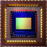
MT9V131C12STC Aptina LLC, MT9V131C12STC Datasheet - Page 10

MT9V131C12STC
Manufacturer Part Number
MT9V131C12STC
Description
SENSOR IMAGE VGA COLOR 48CLCC
Manufacturer
Aptina LLC
Series
Micron®DigitalClarity®r
Type
CMOS Imagingr
Datasheet
1.MT9V131C12STC.pdf
(14 pages)
Specifications of MT9V131C12STC
Package / Case
48-CLCC
Pixel Size
5.6µm x 5.6µm
Active Pixel Array
640H x 480V
Frames Per Second
15 ~ 90
Voltage - Supply
2.8V
Supply Voltage Range
2.55V To 3.05V
Operating Temperature Range
-20°C To +60°C
Digital Ic Case Style
CLCC
No. Of Pins
48
Supply Voltage Max
3.05V
Supply Voltage
RoHS Compliant
Ic Function
Digital Image Sensor
Rohs Compliant
Yes
Lead Free Status / RoHS Status
Lead free / RoHS Compliant
For Use With
557-1243 - KIT HEADBOARD FOR MT9V131557-1242 - KIT DEMO FOR MT9V131
Lead Free Status / RoHS Status
Lead free / RoHS Compliant
Other names
557-1241
Electrical Specifications
Table 5:
PDF: 09005aef824c99b3/Source: 009005aef824c99bb
MT9V131_LDS_2.fm - Rev. B 3/07 EN
I
I
AA
DD
Symbol
Standby Analog standby supply current
Standby Digital standby supply current
V
V
I
V
I
I
I
V
I
I
OH
AA
DD
OL
OZ
OH
IN
OL
IH
IL
DC Electrical Characteristics
V
Input high voltage
Input low voltage
Input leakage current
Output high voltage
Output low voltage
Output high current
Output low current
Tri-state output leakage current
Analog operating supply current
Digital operating supply current
DD
= V
Notes:
AA
Definition
= 2.8 ± 0.25V; T
2. When STANDBY is de-asserted, standby mode is exited immediately (within several master
The recommended die operating temperature ranges from –20°C to +40°C. The sensor
image quality may degrade above +40°C.
1. To place the chip in standby mode, first raise STANDBY to V
cycles before turning off the master clock. Two master clock cycles are required to place the
analog circuitry into standby, low-power mode.
clocks), but the current frame and the next two frames will be invalid. The fourth frame will
contain a valid image.
A
MT9V131: 1/4-Inch SOC VGA CMOS Digital Image Sensor
= 25
°
No pull-up resistor; V
C
Default settings, C
Default settings, C
CLKIN = 12 MHz
CLKIN = 27 MHz
CLKIN = 12 MHz
CLKIN = 27 MHz
STDBY = V
STDBY = V
10
Condition
D
GND
LOAD
LOAD
DD
DD
Micron Technology, Inc., reserves the right to change products or specifications without notice.
IN
= V
= 10pF
= 10pF
DD
or
V
V
DD
DD
Min
10.0
10.0
10.0
–0.3
5.0
0.0
0.0
–5
- 0.25
- 0.2
Electrical Specifications
DD
, then wait two master clock
©2006 Micron Technology, Inc. All rights reserved.
20.0
20.0
15.0
Typ
8.0
2.5
2.5
V
DD
Max
15.0
20.0
25.0
25.0
20.0
20.0
0.8
5.0
0.2
5.0
5.0
5.0
+ 0.25
Preliminary
Unit
mA
mA
mA
mA
µA
µA
µA
µA
V
V
V
V


