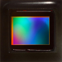
MT9P031I12STM Aptina LLC, MT9P031I12STM Datasheet - Page 7

MT9P031I12STM
Manufacturer Part Number
MT9P031I12STM
Description
SENSOR IMAGE 5MP MONO CMOS 48LCC
Manufacturer
Aptina LLC
Type
CMOS Imagingr
Datasheets
1.MT9P031I12STCH_ES.pdf
(12 pages)
2.MT9P031I12STCH_ES.pdf
(2 pages)
3.MT9P031I12STM.pdf
(12 pages)
Specifications of MT9P031I12STM
Package / Case
48-iLCC
Pixel Size
2.2µm x 2.2µm
Active Pixel Array
2592H x 1944V
Frames Per Second
60
Voltage - Supply
2.6 V ~ 3.1 V
Supply Voltage Range
1.7V To 3.1V, 1.7V To 1.9V, 2.6V To 3.1V
Operating Temperature Range
-30°C To +70°C
Digital Ic Case Style
PLCC
No. Of Pins
48
Supply Voltage Max
3.1V
Ic Function
Digital Image Sensor
Rohs Compliant
Yes
Lead Free Status / RoHS Status
Lead free / RoHS Compliant
For Use With
557-1430 - KIT HEAD BOARD FOR MT9P031557-1429 - KIT DEV FOR MT9P031
Lead Free Status / RoHS Status
Lead free / RoHS Compliant, Lead free / RoHS Compliant
Other names
557-1397
Q3884047
Q3956538
Q4007187
Q3884047
Q3956538
Q4007187
Available stocks
Company
Part Number
Manufacturer
Quantity
Price
Company:
Part Number:
MT9P031I12STM
Manufacturer:
ADI
Quantity:
119
Part Number:
MT9P031I12STM
Manufacturer:
APTINA
Quantity:
20 000
Company:
Part Number:
MT9P031I12STM-DP
Manufacturer:
ON
Quantity:
210
Company:
Part Number:
MT9P031I12STMD ES
Manufacturer:
Aptina LLC
Quantity:
135
Pixel Integration Time Control
Snapshot Mode and Flash Control
Setting Up for Snapshot Mode
Triggering a Snapshot
Strobe Pulse Output
Global Shutter Release Snapshot Mode
Skip and Bin Modes
Smaller Format Resolution
PDF: 09005aef824c997f/Source: 09005aef824c998a
MT9T031_3100_PB_2.fm - Rev. A 8/06 EN
Sensor integration time can be changed by adjusting the amount of time the pixels are
set to collect charge generated from light. The sensor also supports sub-row integration
time for fine control of pixel integration time.
Note that not all integration times may be desired under certain lighting conditions. If
the light source has a flicker component, then the integration time needs to be set prop-
erly to avoid banding in the image.
There are two important signals used for snapshot mode: TRIGGER and STROBE. The
TRIGGER signal initiates the start of a single-frame capture, and STROBE is an output
pulse that may be used to turn on a flash and/or activate a mechanical shutter.
An external trigger signal input allows the snapshot operation to begin after the
TRIGGER pulse moves from a HIGH to LOW state. Alternately, an internal register can
be set through the serial inteface.
After the TRIGGER pulse has signaled a snapshot operation, each row of the imager
array is reset in sequence to clear out any accumulated signal. Once each row of the
imager is reset, the STROBE pulse is output from the imager
In addition to the standard snapshot mode, the MT9T031 has a global shutter release
mode which may be combined with a mechanical shutter to achieve simultaneous
exposure of all rows in the image. Two global shutter modes are available: programmed
exposure and bulb mode.
Row and column skip modes use subsampling to reduce the output resolution without
reducing the field of view. The MT9T031 also has row and column binning modes, which
can reduce the impact of aliasing introduced by the use of skip modes. Both 2X and 3X
binning modes are supported. Rows and columns can be binned independently.
With the flexible windowing capability of the sensor, the user is able to read out different
resolution formats from default of QXGA to UXGA, SXGA, XGA, SVGA, VGA, CIF, QVGA,
QCIF, and so on.
MT9T031: 1/2-Inch 3-Mp Digital Image Sensor
6
Micron Technology, Inc., reserves the right to change products or specifications without notice.
©2006 Micron Technology, Inc. All rights reserved.
Feature Description


