AD9862BSTRL Analog Devices Inc, AD9862BSTRL Datasheet - Page 15
AD9862BSTRL
Manufacturer Part Number
AD9862BSTRL
Description
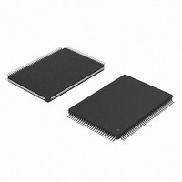
IC FRONT-END MIXED-SGNL 128-LQFP
Manufacturer
Analog Devices Inc
Datasheet
1.AD9860-EBZ.pdf
(32 pages)
Specifications of AD9862BSTRL
Rohs Status
RoHS non-compliant
Rf Type
LMDS, MMDS
Features
12-bit ADC(s), 14-bit DAC(s)
Package / Case
128-LQFP


BIT 5: Q/I Order
This register indicates the order of received complex transmit
data. By default this bit is low, representing I data preceding
Q data. Alternatively, if this bit is set high, the data format is
defined as Q data preceding I data.
BIT 4: Inv TxSync
This register identifies how the first and second data sets are
identified in a complex data set using the TxSYNC bit. By default
this bit is low, and TxSYNC low indicates the first data set is at
the Tx port; TxSYNC high indicates the second data set is at the
Tx port. Setting this bit high inverts the TxSYNC bit. TxSYNC
high indicates the first of the data set, and TxSYNC low indicates
the second of the data set.
BIT 3: Twos Complement
The default data format for Tx data is straight binary. Set this bit
high when providing twos complement Tx data.
BIT 2: Inverse Sample
By default, the transmit data is sampled on the rising edge of the
CLKOUT. Setting this bit high will change this, and the transmit
data will be sampled on the falling edge.
BIT 1: 2 Edges
If the CLKOUT rate is running at half the interleaved data rate,
both edges of the CLKOUT must latch transmit data. Setting
this bit high allows this clocking configuration.
BIT 0: Interleaved
By default, the AD9860/AD9862 powers up in single DAC
operation. If dual transmit data is to be used, the interleaved data
option needs to be enabled by setting this bit high.
REGISTER 19: Tx DIGITAL
BIT 4: 2 Data Paths
Setting this bit high enables both transmit digital paths. By default,
this bit is low and the transmit path utilizes only a single channel.
BIT 3: Keep –ve
This bit configures the Tx Hilbert filter for either positive or nega-
tive frequencies pass band, assuming it is enabled. By default
this bit is low, which selects the positive frequencies. Setting this
bit high will setup the Hilbert filter to pass negative frequencies.
BIT 2: Hilbert
This bit enables or disables the Hilbert filter in the transmit path.
By default, this bit is low, which disables the transmit Hilbert
filter. Setting this bit high enables the transmit Hilbert filter.
BIT 1,0: Interpolation Control
These register bits control the interpolation rate of the transmit
path. Default settings are both bits low, indicating that both inter-
polation filters are bypassed. The MSB and LSB are address D19,
Bits 1 and 0, respectively. Setting binary 01 provides an interpo-
lation rate of 2 ; binary 10 provides an interpolation rate of 4 .
REGISTER 20: Tx MODULATOR
BIT 5: Negative Fine Tune
When this bit is low (default), the Numerically Controlled Oscil-
lator (NCO) provides positive shifts in frequency, assuming fine
modulation is enabled. Setting this bit high will use a negative
frequency shift in the Fine Complex Modulator.
BIT 4: Fine Mode
By default, the NCO and fine modulation stage are bypassed. Setting
this bit high will enable the use of the digital complex modulator,
enabling tuning with the NCO.
REV. 0
–15–
BIT 3: Real Mix Mode
This bit determines if the coarse modulation (controlled by register
Coarse Modulation, will perform a separate real mix on each
channel or a complex mix using the dual channel data. By default,
this bit is set low and a complex mix will be performed. Setting
this bit high will enable the Real Mix mode. Note, the Fine
Modulator Block only performs complex mixing.
BIT 2: Negative Coarse Tune
When this bit is low (default), the coarse modulator provides
positive shifts in frequency. Setting this bit high will shift the coarse
modulator processed data negative in frequency.
BIT 1,0: Coarse Modulation
These bits control what coarse modulation processing will be
performed on the transmit data. A setting of binary 00 (default)
will bypass the modulation block, a setting of binary 01 will shift
the transmit data by f
the transmit data by f
REGISTER 21/22/23: NCO TUNING WORD
FTW [23:0]
These three registers set the 24-bit frequency tuning word (FTW)
for the NCO in the fine modulator stage of the Tx path. The
NCO full-scale tuning word is straight binary and produces
a frequency equivalent to f
REGISTER 24: DLL
BIT 6: Input Clock Control
This bit defines what type of clock will be driving the AD9860/
AD9862. The default state is low, which allows either crystal con-
nected to OSC1 and OSC2 or single-ended reference clock driving
OSC1 to drive the internal timing circuits. If a crystal will not be
used, the internal oscillator should be disabled after power-up
by setting this bit high.
BIT 5: ADC Div2
By default, the ADC is driven directly by the input clock in Normal
Timing Operation mode or the DLL output in the Alternative
Timing Operation mode. Setting this bit high will clock the ADC
at one half the previous clock rate. This is described further in
the timing section.
BIT 4,3: DLL Multiplier
These bits control the DLL multiplication factor. A setting of
binary 00 will bypass the DLL, a setting of binary 01 will multiply
the input clock by 2, and a setting of binary 10 will multiply the
input clock by 4. Default mode is defined by Mode/TxBlank
logic level at power-up or RESET, which configures either Normal
Operation Timing mode or Alternative Timing mode. In Alter-
native Timing mode, the DLL will lock to 4 multiplication
factor (the DLL FAST register remains low by default). If the
Mode/TxBlank pin is low, by default the DLL will be bypassed
and a 1
BIT 2: DLL Power-Down
Setting this register bit high forces the CLK IN multiplier to a
power-down state. This mode can be used to conserve power or
to bypass the internal DLL. To operate the AD9860/AD9862
when the DLL is bypassed, an external clock equal to the fastest
on-chip clock is supplied to the OSC pin(s).
BIT 0: DLL FAST
The DLL can be used to generate output frequencies between
32 MHz to 128 MHz. Because of the large range of locking fre-
quencies allowed, the DLL is separated into two output frequency
ranges, a “slow” range between 32 MHz to 64 MHz and a “fast”
range starting at frequencies above 64 MHz to 128 MHz. By
clock is used internally.
DAC
DAC
/4, and a setting of binary 10 will shift
/8.
DAC
/4 with a resolution of f
AD9860/AD9862
DAC
/2
26
.
Related parts for AD9862BSTRL
Image
Part Number
Description
Manufacturer
Datasheet
Request
R

Part Number:
Description:
BOARD EVALUATION FOR AD9862
Manufacturer:
Analog Devices Inc
Datasheet:

Part Number:
Description:
±1.7g Dual-Axis IMEMS Accelerometer Evaluation Board
Manufacturer:
Analog Devices Inc
Datasheet:
Part Number:
Description:
Inertial Sensor Evaluation System
Manufacturer:
Analog Devices Inc
Datasheet:
Part Number:
Description:
Manufacturer:
Analog Devices Inc
Datasheet:
Part Number:
Description:
Manufacturer:
Analog Devices Inc
Datasheet:
Part Number:
Description:
Manufacturer:
Analog Devices Inc
Datasheet:
Part Number:
Description:
Manufacturer:
Analog Devices Inc
Datasheet:
Part Number:
Description:
Manufacturer:
Analog Devices Inc
Datasheet:
Part Number:
Description:
Manufacturer:
Analog Devices Inc
Datasheet:
Part Number:
Description:
Manufacturer:
Analog Devices Inc
Datasheet:
Part Number:
Description:
Manufacturer:
Analog Devices Inc
Datasheet:
Part Number:
Description:
Manufacturer:
Analog Devices Inc
Datasheet:
Part Number:
Description:
Manufacturer:
Analog Devices Inc
Datasheet: