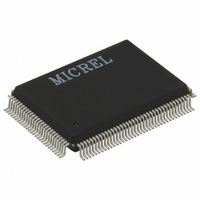
KSZ8995MAI Micrel Inc, KSZ8995MAI Datasheet - Page 20

KSZ8995MAI
Manufacturer Part Number
KSZ8995MAI
Description
IC,Telecom Switching Circuit,CMOS,QFP,128PIN,PLASTIC
Manufacturer
Micrel Inc
Specifications of KSZ8995MAI
Applications
*
Mounting Type
Surface Mount
Package / Case
128-MQFP, 128-PQFP
Number Of Primary Switch Ports
5
Internal Memory Buffer Size
64
Operating Supply Voltage (typ)
Not RequiredV
Fiber Support
Yes
Integrated Led Drivers
Yes
Data Rate
100Mbps
Phy/transceiver Interface
MII/SNI
Power Supply Type
Analog/Digital
Package Type
PQFP
Data Rate (typ)
10/100Mbps
Vlan Support
Yes
Operating Temperature (max)
85C
Operating Temperature (min)
-40C
Pin Count
128
Mounting
Surface Mount
Jtag Support
No
Operating Supply Voltage (max)
Not RequiredV
Operating Supply Voltage (min)
Not RequiredV
Operating Temperature Classification
Industrial
Lead Free Status / RoHS Status
Lead free / RoHS Compliant
For Use With
576-1607 - BOARD EVAL EXPERIMENT KSZ8995MA
Lead Free Status / Rohs Status
Compliant
Other names
576-2126
KSZ8995MAI
KSZ8995MAI
Available stocks
Company
Part Number
Manufacturer
Quantity
Price
Company:
Part Number:
KSZ8995MAI
Manufacturer:
TI
Quantity:
1 700
Company:
Part Number:
KSZ8995MAI
Manufacturer:
MICREL
Quantity:
5
Part Number:
KSZ8995MAI
Manufacturer:
MICREL/麦瑞
Quantity:
20 000
Semptember 2008
Notes:
1.
2.
Pin Number
P = Power supply.
I = Input.
O = Output.
I/O = Bidirectional.
Gnd = Ground.
Ipu = Input w/internal pull-up.
Ipd = Input w/internal pull-down.
Ipd/O = Input w/internal pull-down during reset, output pin otherwise.
Ipu/O = Input w/internal pull-up during reset, output pin otherwise.
Otri = Output tristated.
NC = No connect.
PU = Strap pin pull-up.
PD = Strap pull-down.
Fulld = Full duplex
86
85
78
83
82
81
80
79
75
73
72
71
70
69
74
Pin Name
SMRXDV
SMRXD0
SMRXD1
SMRXD2
SMRXD3
SMTXEN
SMTXER
SCONF1
SMTXD0
SMTXD1
SMTXD2
SMTXD3
SMRXC
SMTXC
SCRS
Type
Ipd/O
Ipd/O
Ipd/O
Ipd/O
Ipd/O
Ipd/O
Ipd
I/O
I/O
Ipd
Ipd
Ipd
Ipd
Ipd
Ipd
(1)
Port
Pin Function
Dual MII configuration pin. For the Switch MII, KSZ8995MA supports
both MAC mode and PHY mode, KSZ8995FQ supports PHY mode
only.
Pin# (91, 86, 87):
000
001
010
011
100
101
110
111
Switch mode carrier sense.
Switch MII receive clock. Input in MAC mode, output in PHY mode MII.
Switch MII receive bit 0; Strap option: LED mode
PD (default) = mode 0; PU = mode 1. See “Register 11.”
LEDX_2
LEDX_1
LEDX_0
Switch MII receive bit 1. Strap option: PD (default) = Switch MII in
100Mbps mode; PU = Switch MII in 10Mbps mode.
Switch MII receive bit 2. Strap option: PD (default) = Switch MII in full-
duplex mode; PU = Switch MII in half-duplex mode.
Switch MII receive bit 3. Strap option: PD (default) = Disable Switch MII
full-duplex flow control; PU = Enable Switch MII full-duplex flow control.
Switch MII receive data valid.
Switch MII transmit clock. Input in MAC mode, output in PHY mode MII.
Switch MII transmit bit 0.
Switch MII transmit bit 1.
Switch MII transmit bit 2.
Switch MII transmit bit 3.
Switch MII transmit enable.
Switch MII transmit error.
20
(2)
Switch MII
Disable, Otri
PHY Mode MII
MAC Mode MII
PHY Mode SNI
Disable
PHY Mode MII
MAC Mode MII
PHY Mode SNI
Fulld/Col
Mode 0
Lnk/Act
Speed
PHY [5] MII
Disable, Otri
Disable, Otri
Disable, Otri
Disable, Otri
Disable
PHY Mode MII
PHY Mode MII
PHY Mode MII
100Lnk/Act
Full duplex
10Lnk/Act
Mode 1
M9999-091508


