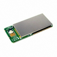
JN5139-001-M/04R1T NXP Semiconductors, JN5139-001-M/04R1T Datasheet - Page 20

JN5139-001-M/04R1T
Manufacturer Part Number
JN5139-001-M/04R1T
Description
JN5139-001-M/SOM041/REEL13 DP
Manufacturer
NXP Semiconductors
Series
JN5139-001-M0xRr
Specifications of JN5139-001-M/04R1T
Frequency
2.4GHz
Modulation Or Protocol
802.15.4 Zigbee
Applications
Home/Building Automation, Industrial Control and Monitoring
Power - Output
19dBm
Sensitivity
-97dBm
Voltage - Supply
2.7 V ~ 3.6 V
Current - Receiving
45mA
Current - Transmitting
120mA
Data Interface
PCB, Surface Mount
Memory Size
96kB RAM, 192kB ROM
Antenna Connector
PCB, Surface Mount
Operating Temperature
-20°C ~ 70°C
Package / Case
Module
Core
RISC
Interface Type
SPI, UART
Core Architecture
RISC
Lead Free Status / RoHS Status
Lead free / RoHS Compliant
Data Rate - Maximum
-
Lead Free Status / Rohs Status
Details
Other names
616-1041-2
935294017534
JN5139-001-M04
JN5139-001-M04R1T
JN5139-001-M04R1T
Q3424158
935294017534
JN5139-001-M04
JN5139-001-M04R1T
JN5139-001-M04R1T
Q3424158
Available stocks
Company
Part Number
Manufacturer
Quantity
Price
Company:
Part Number:
JN5139-001-M/04R1T
Manufacturer:
VTTESSE
Quantity:
156
A.5 Related Documents
[1] IEEE Std 802.15.4-2003 IEEE Standard for Information Technology – Part 15.4 Wireless Medium Access Control
(MAC) and Physical Layer (PHY) Specifications for Low-Rate Wireless Personal Area Networks (LR-WPANs)
[2] JN-DS- JN5139 Wireless Microcontroller Datasheet
[3] JN-RM-2002 802.15.4 Stack API
A.6 Federal Communication Commission Interference Statement
This equipment has been tested and found to comply with the limits for a Class B digital device, pursuant to Part 15
of the FCC Rules. These limits are designed to provide reasonable protection against harmful interference in a
residential installation. This equipment generates, uses, and can radiate radio frequency energy and, if not installed
and used in accordance with the instructions, may cause harmful interference to radio communications. However,
there is no guarantee that interference will not occur in a particular installation. If this equipment does cause harmful
interference to radio or television reception, which can be determined by turning the equipment off and on, the user is
encouraged to try to correct the interference by one of the following measures:
- Reorient or relocate the receiving antenna.
- Increase the separation between the equipment and receiver.
- Connect the equipment into an outlet on a circuit different from that to which the receiver is connected.
- Consult the dealer or an experienced radio/TV technician for help.
This device complies with Part 15 of the FCC Rules. Operation is subject to the following two conditions: (1) This
device may not cause harmful interference, and (2) this device must accept any interference received, including
interference that may cause undesired operation.
FCC Caution: Any changes or modifications not expressly approved by the party responsible for compliance could
void the user's authority to operate this equipment.
WARNING!
FCC Radiation Exposure Statement:
This portable equipment with its antenna complies with FCC’s RF radiation exposure limits set forth for an
uncontrolled environment. To maintain compliance follow the instructions below;
1. This transmitter must not be co-located or operating in conjunction with any other antenna or transmitter.
2. Avoid direct contact to the antenna, or keep it to a minimum while using this equipment.
This transmitter module is authorized to be used in other devices only by OEM integrators under the
following condition:
The transmitter module must not be co-located with any other antenna or transmitter.
As long as the above condition is met, further transmitter testing will not be required. However, the OEM integrator is
still responsible for testing their end product for any additional compliance requirements required with this module
installed (for example, digital device emissions, PC peripheral requirements, etc.).
20
JN-DS-JN5139-xxx-Myy 1v6
© NXP Laboratories UK 2010


