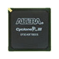
EP3C5E144A7N Altera, EP3C5E144A7N Datasheet - Page 116

EP3C5E144A7N
Manufacturer Part Number
EP3C5E144A7N
Description
Cyclone III
Manufacturer
Altera
Datasheet
1.EP3C5E144A7N.pdf
(274 pages)
Specifications of EP3C5E144A7N
Family Name
Cyclone III
Number Of Logic Blocks/elements
5136
# I/os (max)
94
Frequency (max)
437.5MHz
Process Technology
65nm
Operating Supply Voltage (typ)
1.2V
Logic Cells
5136
Ram Bits
423936
Operating Supply Voltage (min)
1.15V
Operating Supply Voltage (max)
1.25V
Operating Temp Range
-40C to 125C
Operating Temperature Classification
Automotive
Mounting
Surface Mount
Pin Count
144
Package Type
EQFP
Lead Free Status / Rohs Status
Compliant
Available stocks
Company
Part Number
Manufacturer
Quantity
Price
- Current page: 116 of 274
- Download datasheet (6Mb)
6–16
I/O Banks
Figure 6–10. Cyclone III Device Family I/O Banks
Notes to
(1) This is a top view of the silicon die. This is only a graphical representation. For exact pin locations, refer to the pin list and the Quartus II software.
(2) True differential (PPDS, LVDS, mini-LVDS, and RSDS I/O standards) outputs are supported in row I/O banks 1, 2, 5, and 6 only. External resistors
(3) The LVPECL I/O standard is only supported on clock input pins. This I/O standard is not supported on output pins.
(4) The HSTL-12 Class II is supported in column I/O banks 3, 4, 7, and 8 only.
(5) The differential SSTL-18 and SSTL-2, differential HSTL-18, and HSTL-15 I/O standards are supported only on clock input pins and phase-locked
(6) The differential HSTL-12 I/O standard is only supported on clock input pins and PLL output clock pins. Differential HSTL-12 Class II is supported
(7) BLVDS output uses two single-ended outputs with the second output programmed as inverted. BLVDS input uses the LVDS input buffer.
Cyclone III Device Handbook, Volume 1
are needed for the differential outputs in column I/O banks.
loops (PLLs) output clock pins. Differential SSTL-18, differential HSTL-18, and HSTL-15 I/O standards do not support Class II output.
only in column I/O banks 3, 4, 7, and 8.
Figure
f
6–10:
For information about the Cyclone III device family differential PPDS, LVDS,
mini LVDS, RSDS I/O, and Bus LVDS (BLVDS) standard termination, refer to the
High-Speed Differential Interfaces in Cyclone III Devices
I/O pins on the Cyclone III device family are grouped together into I/O banks, and
each bank has a separate power bus. Cyclone III and Cyclone III LS devices have eight
I/O banks, as shown in
bank. All single-ended I/O standards are supported in all banks except HSTL-12
Class II, which is only supported in column I/O banks. All differential I/O standards
are supported in all banks. The only exception is HSTL-12 Class II, which is only
supported in column I/O banks.
I/O Bank 8
I/O Bank 3
(Note
Figure
All I/O Banks Support:
3.3-V LVTTL/LVCMOS
3.0-V LVTTL/LVCMOS
2.5-V LVTTL/LVCMOS
1.8-V LVTTL/LVCMOS
1.5-V LVCMOS
1.2-V LVCMOS
PPDS
LVDS
RSDS
mini-LVDS
Bus LVDS ( 7)
LVPECL (3)
SSTL-2 class I and II
SSTL-18 CLass I and II
HSTL-18 Class I and II
HSTL-15 Class I and II
HSTL-12 Class I and II (4)
Differential SSTL-2 (5)
Differential SSTL-18 (5)
Differential HSTL-18 (5)
Differential HSTL-15 (5)
Differential HSTL-12 (6)
1),
6–10. Each device I/O pin is associated with one I/O
(2)
I/O Bank 4
I/O Bank 7
Chapter 6: I/O Features in the Cyclone III Device Family
chapter.
© December 2009 Altera Corporation
I/O Banks
Related parts for EP3C5E144A7N
Image
Part Number
Description
Manufacturer
Datasheet
Request
R

Part Number:
Description:
Cyclone III Device Data Sheet
Manufacturer:
ALTERA [Altera Corporation]
Datasheet:

Part Number:
Description:
CYCLONE II STARTER KIT EP2C20N
Manufacturer:
Altera
Datasheet:

Part Number:
Description:
CPLD, EP610 Family, ECMOS Process, 300 Gates, 16 Macro Cells, 16 Reg., 16 User I/Os, 5V Supply, 35 Speed Grade, 24DIP
Manufacturer:
Altera Corporation
Datasheet:

Part Number:
Description:
CPLD, EP610 Family, ECMOS Process, 300 Gates, 16 Macro Cells, 16 Reg., 16 User I/Os, 5V Supply, 15 Speed Grade, 24DIP
Manufacturer:
Altera Corporation
Datasheet:

Part Number:
Description:
Manufacturer:
Altera Corporation
Datasheet:

Part Number:
Description:
CPLD, EP610 Family, ECMOS Process, 300 Gates, 16 Macro Cells, 16 Reg., 16 User I/Os, 5V Supply, 30 Speed Grade, 24DIP
Manufacturer:
Altera Corporation
Datasheet:

Part Number:
Description:
High-performance, low-power erasable programmable logic devices with 8 macrocells, 10ns
Manufacturer:
Altera Corporation
Datasheet:

Part Number:
Description:
High-performance, low-power erasable programmable logic devices with 8 macrocells, 7ns
Manufacturer:
Altera Corporation
Datasheet:

Part Number:
Description:
Classic EPLD
Manufacturer:
Altera Corporation
Datasheet:

Part Number:
Description:
High-performance, low-power erasable programmable logic devices with 8 macrocells, 10ns
Manufacturer:
Altera Corporation
Datasheet:

Part Number:
Description:
Manufacturer:
Altera Corporation
Datasheet:

Part Number:
Description:
Manufacturer:
Altera Corporation
Datasheet:

Part Number:
Description:
Manufacturer:
Altera Corporation
Datasheet:


