CY7C4221-15AXC Cypress Semiconductor Corp, CY7C4221-15AXC Datasheet
CY7C4221-15AXC
Specifications of CY7C4221-15AXC
Available stocks


Related parts for CY7C4221-15AXC


CY7C4221-15AXC Summary of contents
Page 1
... Synchronous FIFOs Features High-speed, low-power, first-in first-out (FIFO) memories ■ 64 × 9 (CY7C4421) ❐ 256 × 9 (CY7C4201) ❐ 512 × 9 (CY7C4211) ❐ × 9 (CY7C4221) ❐ × 9 (CY7C4231) ❐ × 9 (CY7C4241) ❐ × 9 (CY7C4251) ❐ High-speed 100 MHz operation (10 ns read/write cycle time) ■ ...
Page 2
Logic Block Diagram WCLK RS Document #: 38-06016 Rev INPUT REGISTER WEN1 WEN2/LD PROGRAM REGISTER Write CONTROL Dual Port RAM Array Write POINTER POINTER RESET LOGIC THREE-ST ATE OUTPUT ...
Page 3
Contents Pin Configuration ............................................................. 4 Architecture ...................................................................... 5 Resetting the FIFO ............................................................ 5 FIFO Operation ................................................................. 5 Programming .................................................................... 5 Programmable Flag (PAE, PAF) Operation ................ 7 Width Expansion Configuration ...................................... 8 Flag Operation .................................................................. 8 Full Flag ....................................................................... 8 ...
Page 4
Pin Configuration PLCC Top View PAF 7 PAE 8 GND 9 REN1 10 RCLK 11 REN2 14151617 181920 Table 1. Pin Definitions Pin Name I/O D Data ...
Page 5
Architecture The CY7C42X1 consists of an array words of nine bits each (implemented by a dual-port array of SRAM cells), a read pointer, a write pointer, control signals (RCLK, WCLK, REN1, REN2, WEN1, WEN2, RS), ...
Page 6
Figure 2. Offset Register Location and Default Values 64 × Empty Offset (LSB) Reg. Default Value = 007h Full Offset (LSB) Reg Default Value = 007h ...
Page 7
... Empty Offset ( default value Full Offset ( default value). Document #: 38-06016 Rev. *F CY7C4421 / 4201 / 4211 / 4221 CY7C4211 (512 – m), CY7C4221 (1K – m), CY7C4231 (2K – m), CY7C4241 (4K – m), and CY7C4251 (8K – m). PAF is set HIGH by the LOW-to-HIGH transition of WCLK when the number of available memory locations is greater than m. ...
Page 8
Width Expansion Configuration Word width may be increased by connecting the corresponding input controls signals of multiple devices. A composite flag should be created for each of the end-point status flags (EF and FF). The partial status flags (PAE and ...
Page 9
Maximum Ratings [4] Exceeding maximum ratings may shorten the useful life of the device. User guidelines are not tested. Storage temperature .................................. –65 Ambient temperature with power applied ............................................. –55 Supply voltage to ground potential ...............–0 +7.0 V ...
Page 10
R1 1.1 K Output C L Including JIG and Equivalent to: Scope Switching Characteristics Over the Operating Range Parameter Description t Clock Cycle Frequency S t Data Access Time A t Clock Cycle Time CLK t Clock ...
Page 11
Switching Waveforms t CLKH WCLK D – WEN1 WEN2 (if applicable) FF [14] t SKEW1 RCLK REN1,REN2 t CLKH RCLK t t ENS ENH REN1,REN2 EF Q – OLZ OE WCLK WEN1 WEN2 Notes 14. ...
Page 12
RS REN1, REN2 WEN1 [17] WEN2/LD EF,PAE FF,PAF Figure 8. First Data Word Latency after Reset with Simultaneous Read and Write WCLK – (First Valid t ENS WEN1 ...
Page 13
WCLK t DS Data Write 1 D – ENH ENS WEN1 WEN2 (if applicable ENS ENH [21] t FRL RCLK t SKEW1 EF REN1 , REN2 LOW OE Data in Output Register Q –Q ...
Page 14
NO Write WCLK [22] t SKEW1 D – WFF FF WEN1 WEN2 (if applicable) RCLK t ENH t ENS REN1, REN2 LOW Data in Output Register Q – Figure 11. Programmable Almost ...
Page 15
... If a write is performed on this rising edge of the write clock, there are Full – (m – 1) words of the FIFO when PAF goes LOW. 27. PAF offset = m. 28. 64-m words for CY7C4421, 256 – m words in FIFO for CY7C4201, 512 – m words for CY7C4211, 1024 – m words for CY7C4221, 2048 – m words for CY7C4231, 4096 – m words for CY7C4241, 8192 – m words for CY7C4251. ...
Page 16
CLK t CLKH RCLK t ENS WEN2/LD t ENS REN1, REN2 Q – Document #: 38-06016 Rev. *F CY7C4421 / 4201 / 4211 / 4221 Figure 14. Read Programmable Registers t CLKL t ENH t A Unknown ...
Page 17
Typical AC and DC Characteristics Normalized Supply Current vs. Supply Voltage 1.4 1 25C 0 100 MHz 0.6 4 4.5 5 5.5 6 Supply Voltage (V) Normalized t vs. Supply ...
Page 18
... Ordering Information Synchronous FIFO Speed (ns) Ordering Code 15 CY7C4221-15AXC CY7C4221-15JXC Synchronous FIFO Speed (ns) Ordering Code 15 CY7C4231-15AXC CY7C4231-15JXC Ordering Code Definition Document #: 38-06016 Rev. *F CY7C4421 / 4201 / 4211 / 4221 Package Name Package Type A32 32-Pin Pb-free thin quad flatpack J65 32-Pin Pb-free plastic leaded chip carrier ...
Page 19
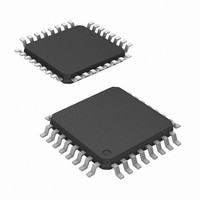
Package Diagrams Figure 15. 32-Pin Pb-free Thin Plastic Quad Flatpack 7 × 7 × 1.0 mm A32, 51-85063 9.00±0.25 SQ 7.00±0. SEATING PLANE 1.20 MAX. 0.08 0.20 MAX. Document #: 38-06016 Rev. *F CY7C4421 / ...
Page 20
Package Diagrams Figure 16. 32-Pin Pb-free Plastic Leaded Chip Carrier J65, 51-85002 Document #: 38-06016 Rev. *F CY7C4421 / 4201 / 4211 / 4221 CY7C4231 / 4241 / 4251 51-85002 *C Page [+] Feedback ...
Page 21
Acronyms Table 4. Acronyms Used Acronym Description CMOS complementary metal oxide semiconductor CE chip enable I/O input/output OE output enable SRAM static random access memory TSOP thin small outline package WE write enable Document #: 38-06016 Rev. *F CY7C4421 / ...
Page 22
... Change Input Leakage current I RBI Power up requirements added to Maximum Ratings Information ESH Added Pb-free logo to top of front page Added CY7C4421-10JXC, CY7C4201-15AXC. CY7C4201-15JXC, CY7C4211-10AXI, CY7C4211-15AXC, CY7C4211-15JXC, CY7C4221-15AXC, CY7C4221-15JXC, CY7C4231-15JXC, CY7C4231-15AXC, CY7C4241-10AXC, CY7C4241-15AXC, CY7C4241-15JXC, CY7C4251-10JXC, CY7C4251-10AXI, CY7C4251-15AXC, CY7C4251-15JXC Added Table of Contents Updated TQFP package diagram Removed inactive parts from Ordering information and updated package diagram ...
Page 23
... Cypress against all charges. Any Source Code (software and/or firmware) is owned by Cypress Semiconductor Corporation (Cypress) and is protected by and subject to worldwide patent protection (United States and foreign), United States copyright laws and international treaty provisions. Cypress hereby grants to licensee a personal, non-exclusive, non-transferable license to copy, use, modify, create derivative works of, and compile the Cypress Source Code and derivative works for the sole purpose of creating custom software and or firmware in support of licensee product to be used only in conjunction with a Cypress integrated circuit as specified in the applicable agreement ...