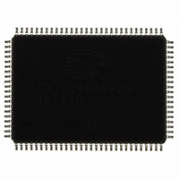
CY7C1460AV25-167AXC Cypress Semiconductor Corp, CY7C1460AV25-167AXC Datasheet - Page 10

CY7C1460AV25-167AXC
Manufacturer Part Number
CY7C1460AV25-167AXC
Description
SRAM (Static RAM)
Manufacturer
Cypress Semiconductor Corp
Datasheet
1.CY7C1460AV25-167BZC.pdf
(29 pages)
Specifications of CY7C1460AV25-167AXC
Format - Memory
RAM
Memory Type
SRAM - Synchronous
Memory Size
36M (1M x 36)
Speed
167MHz
Interface
Parallel
Voltage - Supply
2.375 V ~ 2.625 V
Operating Temperature
0°C ~ 70°C
Package / Case
100-LQFP
Lead Free Status / RoHS Status
Lead free / RoHS Compliant
Other names
428-2162
CY7C1460AV25-167AXC
CY7C1460AV25-167AXC
Available stocks
Company
Part Number
Manufacturer
Quantity
Price
Company:
Part Number:
CY7C1460AV25-167AXC
Manufacturer:
Cypress Semiconductor Corp
Quantity:
135
Company:
Part Number:
CY7C1460AV25-167AXC
Manufacturer:
MURATA
Quantity:
30 000
Company:
Part Number:
CY7C1460AV25-167AXC
Manufacturer:
Cypress Semiconductor Corp
Quantity:
10 000
Company:
Part Number:
CY7C1460AV25-167AXCT
Manufacturer:
Cypress Semiconductor Corp
Quantity:
10 000
Truth Table
Document Number: 38-05354 Rev. *G
Deselect cycle
Continue deselect cycle
Read cycle (begin burst)
Read cycle (continue burst)
NOP/dummy read (begin burst)
Dummy read (continue burst)
Write cycle (begin burst)
Write cycle (continue burst)
NOP/WRITE ABORT (begin burst)
WRITE ABORT (continue burst)
IGNORE CLOCK EDGE (stall)
Sleep MODE
Notes
1. X = “Don't Care”, H = Logic HIGH, L = Logic LOW, CE stands for all chip enables active. BWx = L signifies at least one byte write select is active, BWx = valid
2. Write is defined by WE and BW
3. When a write cycle is detected, all I/Os are tri-stated, even during byte writes.
4. The DQ and DQP pins are controlled by the current cycle and the OE signal.
5. CEN = H inserts wait states.
6. Device will power-up deselected and the I/Os in a tri-state condition, regardless of OE.
7. OE is asynchronous and is not sampled with the clock rise. It is masked internally during write cycles. During a read cycle DQ
signifies that the desired byte write selects are asserted, see Write Cycle Description table for details.
OE is inactive or when the device is deselected, and DQ
Operation
[1, 2, 3, 4, 5, 6, 7]
X
. See Write Cycle Description table for details.
None
None
External
Next
External
Next
External
Next
None
Next
Current
None
Address
Used
s
=data when OE is active.
CE
H
X
X
X
X
X
X
X
L
L
L
L
ZZ
H
L
L
L
L
L
L
L
L
L
L
L
ADV/LD
H
H
H
H
H
X
L
L
L
L
L
X
WE
X
X
H
X
H
X
X
X
X
X
L
L
BW
X
H
H
X
X
X
X
X
X
L
L
X
x
OE CEN CLK
X
X
H
H
X
X
X
X
X
X
L
L
s
H
X
and DQP
L
L
L
L
L
L
L
L
L
L
CY7C1460AV25
CY7C1462AV25
CY7C1464AV25
L-H
L-H
L-H Data out (Q)
L-H Data out (Q)
L-H
L-H
L-H
L-H
L-H
L-H
L-H
X
X
= Three-state when
Data in (D)
Data in (D)
Tri-state
Tri-state
Tri-state
Tri-state
Tri-state
Tri-state
Tri-state
Page 10 of 29
DQ
–
[+] Feedback


