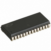
CY7C1399BN-15VXA Cypress Semiconductor Corp, CY7C1399BN-15VXA Datasheet - Page 5

CY7C1399BN-15VXA
Manufacturer Part Number
CY7C1399BN-15VXA
Description
CY7C1399BN-15VXA
Manufacturer
Cypress Semiconductor Corp
Datasheet
1.CY7C1399BN-12ZXC.pdf
(8 pages)
Specifications of CY7C1399BN-15VXA
Format - Memory
RAM
Memory Type
SRAM - Asynchronous
Memory Size
256K (32K x 8)
Speed
15ns
Interface
Parallel
Voltage - Supply
3 V ~ 3.6 V
Operating Temperature
-40°C ~ 85°C
Package / Case
28-SOJ
Density
256Kb
Access Time (max)
15ns
Sync/async
Asynchronous
Architecture
SDR
Clock Freq (max)
Not RequiredMHz
Operating Supply Voltage (typ)
3.3V
Address Bus
15b
Package Type
SOJ
Operating Temp Range
-40C to 85C
Number Of Ports
1
Supply Current
50mA
Operating Supply Voltage (min)
3V
Operating Supply Voltage (max)
3.6V
Operating Temperature Classification
Industrial
Mounting
Surface Mount
Pin Count
28
Word Size
8b
Number Of Words
32K
Lead Free Status / RoHS Status
Lead free / RoHS Compliant
Lead Free Status / RoHS Status
Lead free / RoHS Compliant
Other names
428-2012-5
Document #: 001-06490 Rev. *C
Switching Waveforms
Write Cycle No. 1 (WE Controlled)
Write Cycle No. 2 (CE Controlled)
Write Cycle No. 3 (WE Controlled, OE LOW)
Notes:
13. Data I/O is high impedance if OE = V
14. If CE goes HIGH simultaneously with WE HIGH, the output remains in a high-impedance state.
15. During this period, the I/Os are in the output state and input signals should not be applied.
ADDRESS
ADDRESS
ADDRESS
DATA I/O
DATA I/O
DATA I/O
CE
WE
WE
WE
CE
OE
CE
NOTE 15
NOTE 15
t
SA
(continued)
IH
t
SA
.
t
HZOE
[8, 13, 14]
t
[8, 13, 14]
HZWE
t
SA
[9, 14]
t
AW
t
AW
t
AW
t
WC
t
t
WC
WC
DATA
t
PWE
t
SD
DATA
DATA
IN
t
SCE
t
SD
t
VALID
SD
IN
IN
VALID
VALID
t
HD
t
t
t
HA
HA
LZWE
t
HA
t
t
HD
HD
CY7C1399BN
Page 5 of 8
[+] Feedback


