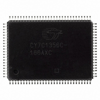
CY7C1356C-166AXCT Cypress Semiconductor Corp, CY7C1356C-166AXCT Datasheet - Page 14

CY7C1356C-166AXCT
Manufacturer Part Number
CY7C1356C-166AXCT
Description
CY7C1356C-166AXCT
Manufacturer
Cypress Semiconductor Corp
Datasheet
1.CY7C1354C-166AXC.pdf
(32 pages)
Specifications of CY7C1356C-166AXCT
Format - Memory
RAM
Memory Type
SRAM - Synchronous
Memory Size
9M (512K x 18)
Speed
166MHz
Interface
Parallel
Voltage - Supply
3.135 V ~ 3.6 V
Operating Temperature
0°C ~ 70°C
Package / Case
100-LQFP
Lead Free Status / RoHS Status
Lead free / RoHS Compliant
Available stocks
Company
Part Number
Manufacturer
Quantity
Price
Company:
Part Number:
CY7C1356C-166AXCT
Manufacturer:
Cypress Semiconductor Corp
Quantity:
10 000
To guarantee that the boundary scan register captures the
correct value of a signal, the SRAM signal must be stabilized
long enough to meet the TAP controller's capture setup plus hold
times (t
correctly if there is no way in a design to stop (or slow) the clock
during a SAMPLE/PRELOAD instruction. If this is an issue, it is
still possible to capture all other signals and simply ignore the
value of the CK and CK# captured in the boundary scan register.
After the data is captured, it is possible to shift out the data by
putting the TAP into the Shift-DR state. This places the boundary
scan register between the TDI and TDO pins.
PRELOAD enables an initial data pattern to be placed at the
latched parallel outputs of the boundary scan register cells prior
to the selection of another boundary scan test operation.
TAP Timing
TAP AC Switching Characteristics
Over the Operating Range
Document Number: 38-05538 Rev. *L
Clock
t
t
t
t
Output Times
t
t
Setup Times
t
t
t
Hold Times
t
t
t
Notes
Parameter
TCYC
TF
TH
TL
TDOV
TDOX
TMSS
TDIS
CS
TMSH
TDIH
CH
14. t
15. Test conditions are specified using the load in TAP AC test Conditions. t
CS
and t
CS
and t
CH
refer to the setup and hold time requirements of latching data from the boundary scan register.
TCK clock cycle time
TCK clock frequency
TCK clock HIGH time
TCK clock LOW time
TCK clock LOW to TDO valid
TCK clock LOW to TDO invalid
TMS setup to TCK clock rise
TDI setup to TCK clock rise
Capture setup to TCK rise
TMS hold after TCK clock rise
TDI hold after clock rise
Capture hold after clock rise
CH
Test M ode Select
). The SRAM clock input might not be captured
Test Data-Out
Test Data-In
Test Clock
[14, 15]
(TM S)
(TDO)
(TCK )
(TDI)
1
Description
t TM SS
t TDIS
2
t TM SH
t TDIH
t TH
DON’T CA RE
t
TL
R
/t
F
3
= 1 ns.
t CY C
The shifting of data for the SAMPLE and PRELOAD phases can
occur concurrently when required - that is, while data captured
is shifted out, the preloaded data can be shifted in.
BYPASS
When the BYPASS instruction is loaded in the instruction register
and the TAP is placed in a Shift-DR state, the bypass register is
placed between the TDI and TDO balls. The advantage of the
BYPASS instruction is that it shortens the boundary scan path
when multiple devices are connected together on a board.
Reserved
These instructions are not implemented but are reserved for
future use. Do not use these instructions.
UNDEFINED
4
t TDOX
t TDOV
5
CY7C1354C, CY7C1356C
Min
50
20
20
–
–
0
5
5
5
5
5
5
6
Max
20
10
–
–
–
–
–
–
–
–
–
–
Page 14 of 32
Unit
MHz
ns
ns
ns
ns
ns
ns
ns
ns
ns
ns
ns
[+] Feedback


