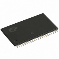
CY7C1041D-10ZSXIT Cypress Semiconductor Corp, CY7C1041D-10ZSXIT Datasheet

CY7C1041D-10ZSXIT
Specifications of CY7C1041D-10ZSXIT
Related parts for CY7C1041D-10ZSXIT
CY7C1041D-10ZSXIT Summary of contents
Page 1
... HIGH), the BHE and BLE are disabled (BHE, BLE HIGH), or during a write operation (CE LOW, and WE LOW). The CY7C1041D is available in a standard 44-pin 400-mil-wide body width SOJ and 44-pin TSOP II package with center power and ground (revolutionary) pinout. ...
Page 2
... Data Retention Waveform ................................................ 6 Document #: 38-05472 Rev. *F Switching Waveforms ...................................................... 7 Truth Table ...................................................................... 10 Ordering Information ...................................................... 10 Ordering Code Definitions ......................................... 10 Package Diagrams .......................................................... 11 Acronyms ........................................................................ 12 Document Conventions ................................................. 12 Units of Measure ....................................................... 12 Document History Page ................................................. 13 Sales, Solutions, and Legal Information ...................... 14 Worldwide Sales and Design Support ....................... 14 Products .................................................................... 14 PSoC Solutions ......................................................... 14 CY7C1041D Page [+] Feedback ...
Page 3
... I/O I I/O I I/O I Static Discharge Voltage............ ...............................>2001 V (per MIL-STD-883, Method 3015) Latch-up Current...................................................... >200 mA Operating Range ...–0 +6.0 V Range +0 Industrial +0 Automotive CY7C1041D Ambient V Speed CC Temperature 5 V ± 0.5 –40°C to +85° ± 0.5 –40°C to +125° Page [+] Feedback ...
Page 4
... < MAX , CE > V – 0 > V – 0 < 0 Test Conditions T = 25° MHz 5 Test Conditions Still Air, soldered × 4.5 inch, four-layer printed circuit board CY7C1041D -12 (Automotive) Max Min Max Unit 2.4 V 0.4 0 0 0.8 –0.5 0.8 V μA +1 –1 +1 μA +1 –1 ...
Page 5
... CC is less than less than less than t HZCE LZCE HZOE LZOE HZBE CY7C1041D ALL INPUT PULSES 90% 90% 10% 10% ≤ (b) THÉ VENIN EQUIVALENT 167Ω 1.73 V –12 (Automotive) Max Min Max Unit μs 100 ...
Page 6
... Min Over the Operating Range [13] Conditions 2 > V – 0 > V – 0 < 0 DATA RETENTION MODE 4 > CDR and t HZWE > 50 μs or stable at V > 50 μ CC(Min) CC(Min CY7C1041D –12 (Automotive) Max Min Max Unit Min Max Unit 2.0 V Ind’ Auto 4.5 V ...
Page 7
... CE t ACE OE t DOE BHE, BLE t LZOE t DBE t LZBE HIGH IMPEDANCE DATA OUT t LZCE SUPPLY CURRENT Document #: 38-05472 Rev. *F [13, 14] Figure 2. Read Cycle No OHA t RC DATA VALID 50% CY7C1041D DATA VALID [15,16] t HZOE t HZCE t HZBE HIGH IMPEDANCE t PD ICC 50% ISB Page [+] Feedback ...
Page 8
... WE is HIGH for read cycle. 16. Address valid prior to or coincident with CE transition LOW 17. Data I/O is high impedance BHE and/or BLE goes HIGH simultaneously with WE going HIGH, the output remains in a high-impedance state. Document #: 38-05472 Rev. *F [17, 18 SCE PWE PWE t SCE CY7C1041D Page [+] Feedback ...
Page 9
... BHE, BLE ADDRESS BHE, BLE DATA I/O NOTE Note 19. During this period the I/Os are in the output state and input signals should not be applied. Document #: 38-05472 Rev SCE PWE t SD DATA VALID SCE PWE HZWE SD 19 CY7C1041D [16, 17 LZWE Page [+] Feedback ...
Page 10
... Ordering Information Table 1 lists the CY7C1041D key package features and ordering codes. The table contains only the parts that are currently available. If you do not see what you are looking for, contact your local sales representative. For more information, visit the Cypress website at www ...
Page 11
... Package Diagrams Figure 8. 44-Pin (400-Mil) Molded SOJ (51-85082) Document #: 38-05472 Rev. *F Figure 9. 44-pin TSOP II (51-85087) CY7C1041D 51-85082 *C 51-85087 *B 51-85087 *C Page [+] Feedback ...
Page 12
... Thin Small Outline Package VFBGA Very Fine-Pitch Ball Grid Array Document #: 38-05472 Rev. *F Document Conventions Units of Measure Symbol Unit of Measure ns nano seconds V Volts µA micro Amperes mA milli Amperes mV milli Volts mW milli Watts MHz Mega Hertz pF pico Farad °C degree Celcius W Watts CY7C1041D Page [+] Feedback ...
Page 13
... Document History Page Document Title: CY7C1041D 4-Mbit (256K x 16) Static RAM Document Number: 38-05472 Orig. of Submission Revision ECN Change ** 201560 SWI *A 233729 RKF *B 351117 PCI *C 446328 NXR *D 2897049 VKN *E 3109184 AJU 12/13/2010 Added *F 3236731 PRAS 04/21/2011 Template updates. Document #: 38-05472 Rev. *F ...
Page 14
... Cypress against all charges. Use may be limited by and subject to the applicable Cypress software license agreement. Document #: 38-05472 Rev. *F All products and company names mentioned in this document may be the trademarks of their respective holders. cypress.com/go/plc Revised April 21, 2011 CY7C1041D PSoC Solutions psoc.cypress.com/solutions PSoC 1 | PSoC 3 ...


