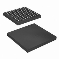
CY7B994V-5BBXC Cypress Semiconductor Corp, CY7B994V-5BBXC Datasheet - Page 12

CY7B994V-5BBXC
Manufacturer Part Number
CY7B994V-5BBXC
Description
IC,Eighteen Distributed-Output Clock Driver,BGA,100PIN,PLASTIC
Manufacturer
Cypress Semiconductor Corp
Series
RoboClock™r
Type
Clock Buffer, Fanout Distributionr
Datasheet
1.CY7B993V-2AXC.pdf
(18 pages)
Specifications of CY7B994V-5BBXC
Pll
Yes
Input
LVPECL, LVTTL
Output
LVTTL
Number Of Circuits
1
Ratio - Input:output
4:18
Differential - Input:output
No/No
Frequency - Max
200MHz
Divider/multiplier
Yes/Yes
Voltage - Supply
2.97 V ~ 3.63 V
Operating Temperature
0°C ~ 70°C
Mounting Type
Surface Mount
Package / Case
100-LBGA
Frequency-max
200MHz
Lead Free Status / RoHS Status
Lead free / RoHS Compliant
Available stocks
Company
Part Number
Manufacturer
Quantity
Price
Company:
Part Number:
CY7B994V-5BBXC
Manufacturer:
Cypress Semiconductor Corp
Quantity:
10 000
Company:
Part Number:
CY7B994V-5BBXCT
Manufacturer:
Cypress Semiconductor Corp
Quantity:
10 000
Switching Characteristics
Notes
Document #: 38-07127 Rev. *I
TTB
t
t
t
t
t
t
t
t
t
t
t
t
t
18. TTB is the window between the earliest and the latest output clocks with respect to the input reference clock across variations in output frequency, supply voltage,
19. Tested initially and after any design or process changes that may affect these parameters.
20. Rise and fall times are measured between 2.0V and 0.8V.
21. f
22. t
23. UI = Unit Interval. Examples: 1 UI is a full period. 0.1UI is 10% of period.
24. Measured at 0.5V deviation from starting voltage.
25. For t
26. These figures are for illustrations only. The actual ATE loads may vary.
Parameter
PDDELTA
REFpwh
REFpwl
r
LOCK
RELOCK1
RELOCK2
ODCV
PWH
PWL
PDEV
OAZ
OAZ
/t
f
operating temperature, input clock edge rate, and process. The measurements are taken with the AC test load specified and include output-output skew, cycle-cycle
jitter, and dynamic phase error. TTB is equal to or smaller than the maximum specified value at a given frequency.
NOM
PWH
OZA
must be within the frequency range defined by the same FS state.
is measured at 2.0V. t
minimum, C
Total Timing Budget window (same frequency and phase)
18]
Propagation Delay difference between two devices
REF input (Pulse Width HIGH)
REF input (Pulse Width LOW)
Output Rise/Fall Time
PLL Lock Time from Power up
PLL Relock Time (from same frequency, different phase)
with Stable Power Supply
PLL Relock Time (from different frequency, different phase)
with Stable Power Supply
Output duty cycle deviation from 50%
Output HIGH time deviation from 50%
Output LOW time deviation from 50%
Period deviation when changing from reference to
reference
DIS[1:4]/FBDIS HIGH to output high impedance from
ACTIVE
DIS[1:4]/FBDIS LOW to output ACTIVE from output high
impedance
For LOCK output only
R1 = 910
R2 = 910
C
L
< 30 pF
L
= 0 pF. For t
(Includes fixture and
probe capacitance)
[14, 24]
[23]
PWL
[24, 25]
is measured at 0.8V.
OZA
maximum, C
[20]
For all other outputs
R1 = 100
R2 = 100
C
Description
L
Over the Operating Range
[21]
< 25 pF to 185 MHz
GND
3.3V
Figure 5. AC Test Loads and Waveform
[19]
L
or 10 pF at 200 MHz
< 1 ns
[19]
= 25 pF to 185 MHz or 10 pF to 200 MHz.
(a) LVTTL AC Test Load
(b) TTL Input Test Waveform
[13]
[22]
[22]
0.8V
2.0V
OUTPUT
[9, 10, 11, 12, 13]
[17]
[17,
C
L
0.15
–1.0
Min
2.0
2.0
1.0
0.5
–
–
–
–
–
–
–
–
CY7B993/4V-2
3.3V
(continued)
Typ
2.0V
–
–
–
–
–
–
[26]
R1
R2
0.8V
< 1 ns
0.025
1000
Max
500
200
500
2.0
1.0
1.5
2.0
10
10
14
–
–
CY7B993V, CY7B994V
0.15
–1.0
Min
2.0
2.0
1.0
0.5
–
–
–
–
–
–
–
–
CY7B993/4V-5
Typ
–
–
–
–
–
–
RoboClock
0.025
1000
Max
700
200
500
2.0
1.0
1.5
2.0
10
10
14
–
–
Page 12 of 18
Unit
ms
s
s
ps
ps
ns
ns
ns
ns
ns
ns
UI
ns
ns
[+] Feedback


