CY7B994V-5BBC Cypress Semiconductor Corp, CY7B994V-5BBC Datasheet
CY7B994V-5BBC
Specifications of CY7B994V-5BBC
Available stocks


Related parts for CY7B994V-5BBC


CY7B994V-5BBC Summary of contents
Page 1
... Document #: 38-07127 Rev. *I High Speed Multi Phase PLL Clock Buffer Functional Description The CY7B993V and CY7B994V High-speed Multi-phase PLL Clock Buffers offer user selectable control over system clock functions. This multiple output clock driver provides the system integrator with functions necessary to optimize the timing of high-performance computer and communication systems ...
Page 2
... Select 3 2DS1 Matrix DIS2 1F0 3 Divide and 1F1 3 Phase 3 1DS0 Select 1DS1 3 Matrix DIS1 RoboClock CY7B993V, CY7B994V LOCK Control Logic Divide and Phase Generator QFA0 QFA1 4QA0 4QA1 4QB0 4QB1 3QA0 3QA1 3QB0 3QB1 2QA0 2QA1 2QB0 2QB1 1QA0 1QA1 ...
Page 3
... Divide and Phase Select Matrix .................................... 7 Output Disable Description............................................ 8 INV3 Pin Function ......................................................... 9 Lock Detect Output Description..................................... 9 Factory Test Mode Description ..................................... 9 Safe Operating Zone ..................................................... 9 Document #: 38-07127 Rev. *I CY7B993V, CY7B994V Absolute Maximum Conditions ........................................10 Operating Range ................................................................10 Electrical Characteristics...................................................10 Switching Characteristics .................................................11 AC Timing Diagrams ..........................................................13 Ordering Information .........................................................14 Package Diagrams ...
Page 4
... VCCQ 20 4DS0 21 3DS0 22 2DS0 23 1DS0 24 GND Document #: 38-07127 Rev. *I Figure 1. Pin Diagram – 100-Pin TQFP CY7B993/ RoboClock CY7B993V, CY7B994V VCCQ 74 REFA+ 73 REFA – 72 REFSEL 71 REFB– 70 REFB+ 69 2F0 GND 66 2QA0 65 VCCN 64 2QA1 63 GND 62 GND 61 2QB0 60 VCCN 59 2QB1 58 GND 57 FBF0 56 1F0 ...
Page 5
... DIS1 VCCN VCCN GND (3_level) VCCN 3QA0 3QA1 GND 3QB0 Pin Description 2). Table , LOW indicates a connection to GND, and MID indicates an open connection. Internal termination CC RoboClock CY7B993V, CY7B994V FBKA– FBKA+ FBSEL REFA+ GND REFA– VCCN REFB+ VCCN 2QA0 1F0 2QA1 ...
Page 6
... VCO frequency. There are two NOM versions: a low-speed device (CY7B993V) where f from 12 MHz to 100 MHz, and a high-speed device (CY7B994V) that ranges from 24 MHz to 200 MHz. The FS setting for each device is shown in The f frequency is seen on “divide-by-one” outputs. For the ...
Page 7
... U an output programmed with 8t 16t with respect to REF the V and Phase Generator. f NOM CO when the output connected undivided. NOM RoboClock CY7B993V, CY7B994V Output Skew Function Feed- Bank1 Bank2 Bank3 Bank4 –4t –4t –8t – –3t – ...
Page 8
... HIGH. When disabled to the HOLD-OFF Note 4. FB connected to an output selected for “Zero” skew (i.e., FBF0 = MID or XF[1:0] = MID). Document #: 38-07127 Rev. *I CY7B993V, CY7B994V [] state, non-inverting outputs are driven to a logic LOW state on its falling edge. Inverting outputs are driven to a logic HIGH state on its rising edge ...
Page 9
... When in factory test mode (OUTPUT_MODE = MID), the device can be reset to a deterministic state by driving the DIS4 input Document #: 38-07127 Rev. *I CY7B993V, CY7B994V HIGH. When the DIS4 input is driven HIGH in factory test mode, all clock outputs go to High Z; after the selected reference clock pin has five positive transitions, all the internal finite state machines (FSM) are set to a deterministic state ...
Page 10
... Max GND CC IN Min < V < Max CC Min < V < Max CC Min < V < Max GND IN RoboClock CY7B993V, CY7B994V V CC 3.3V 10 +70 C 3.3V 10 +85 C Min Max Unit 2.4 – V 2.4 – V – 0.5 V – 0.5 V ...
Page 11
... Bank1 and FB Bank configured to run at maximum frequency (f CCI CY7B994V), and all other clock output banks to run at half the maximum frequency. FS and OUTPUT_MODE are asserted to the HIGH state. 8. This is dependent upon frequency and number of outputs of a bank being loaded. The value indicates maximum I load terminated to 50 ...
Page 12
... Figure 5. AC Test Loads and Waveform 3.3V OUTPUT 200 MHz (a) LVTTL AC Test Load 3.3V 2.0V 0.8V < (b) TTL Input Test Waveform = 185 MHz 200 MHz. L RoboClock CY7B993V, CY7B994V CY7B993/4V-5 Unit Typ Max Min Typ Max – 500 – – 700 ps – ...
Page 13
... PD FB DEVICE1 t PDELTA t PDELTA FB DEVICE2 Q t SKEW2 t SKEW2 INVERTED Q Document #: 38-07127 Rev. *I QFA0 or [1:4]Q[A:B]0 t SKEWPR t PWL QFA1 or [1:4]Q[A:B]1 0.8V t [1:4]QA[0:1] CCJ1-3,4-12 t SKEWBNK [1:4]QB[0: SKEW0,1 Other Q COMPLEMENTARY A COMPLEMENTARY B RoboClock CY7B993V, CY7B994V t SKEWPR t SKEWBNK t ODCV t ODCV t SKEW0,1 t SKEWCPR crossing crossing Page [+] Feedback ...
Page 14
... Ordering Information Propagation Max Speed Ordering Code Delay (ps) (MHz) 250 200 CY7B994V-2BBI 250 200 CY7B994V-2BBIT 500 200 CY7B994V-5BBC 500 200 CY7B994V-5BBCT Pb-free 250 100 CY7B993V-2AXC 250 100 CY7B993V-2AXCT 250 100 CY7B993V-2AXI 250 200 CY7B994V-2AXC 250 200 CY7B994V-2AXCT 250 200 CY7B994V-2BBXC 250 ...
Page 15
... Package Diagrams Figure 6. 100-Pin Thin Plastic Quad Flat Pack (TQFP) A100 Document #: 38-07127 Rev. *I RoboClock CY7B993V, CY7B994V 51-85048 *D Page [+] Feedback ...
Page 16
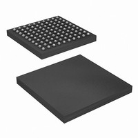
... Package Diagrams (continued) Figure 7. 100-Ball Thin Ball Grid Array ( 1.4 mm) BB100 Document #: 38-07127 Rev. *I RoboClock CY7B993V, CY7B994V 51-85107 *C Page [+] Feedback ...
Page 17
... Changed from Spec number: 38-00747 to 38-07127 Added three industrial packages Added TTB Features Power up requirements to operating conditions information Added Min F value of 12 MHz for CY7B993V and 24 MHz for CY7B994V to out switching characteristics table Corrected prop delay limit parameter from (t Output Description paragraph ...
Page 18
... TTB™ trademark and RoboClock and PSoC are the registered trademarks of Cypress Semiconductor Corp. All other trademarks or registered trademarks referenced herein are property of the respective corporations. cypress.com/go/plc Revised November 02, 2010 RoboClock CY7B993V, CY7B994V PSoC Solutions psoc.cypress.com/solutions PSoC 1 | PSoC 3 | PSoC 5 Page ...