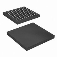
CY7B994V-2BBI Cypress Semiconductor Corp, CY7B994V-2BBI Datasheet - Page 8

CY7B994V-2BBI
Manufacturer Part Number
CY7B994V-2BBI
Description
IC,Sixteen Distributed-Output Clock Driver,BGA,100PIN,PLASTIC
Manufacturer
Cypress Semiconductor Corp
Series
RoboClock™r
Type
Clock Buffer, Fanout Distributionr
Datasheet
1.CY7B993V-2AXC.pdf
(18 pages)
Specifications of CY7B994V-2BBI
Pll
Yes
Input
LVPECL, LVTTL
Output
LVTTL
Number Of Circuits
1
Ratio - Input:output
4:18
Differential - Input:output
No/No
Frequency - Max
200MHz
Divider/multiplier
Yes/Yes
Voltage - Supply
2.97 V ~ 3.63 V
Operating Temperature
-40°C ~ 85°C
Mounting Type
Surface Mount
Package / Case
100-LBGA
Frequency-max
200MHz
Number Of Elements
1
Supply Current
250mA
Pll Input Freq (min)
24MHz
Pll Input Freq (max)
200MHz
Operating Supply Voltage (typ)
3.3V
Operating Temp Range
-40C to 85C
Package Type
BGA
Output Frequency Range
24 to 200MHz
Operating Supply Voltage (min)
2.97V
Operating Supply Voltage (max)
3.63V
Operating Temperature Classification
Industrial
Pin Count
100
Lead Free Status / RoHS Status
Contains lead / RoHS compliant by exemption
Lead Free Status / RoHS Status
Contains lead / RoHS compliant by exemption
Available stocks
Company
Part Number
Manufacturer
Quantity
Price
Company:
Part Number:
CY7B994V-2BBI
Manufacturer:
Maxim
Quantity:
54
Company:
Part Number:
CY7B994V-2BBI
Manufacturer:
CYPRESS
Quantity:
1 045
Company:
Part Number:
CY7B994V-2BBI
Manufacturer:
Cypress Semiconductor Corp
Quantity:
10 000
Part Number:
CY7B994V-2BBI
Manufacturer:
CYPRESS/赛普拉斯
Quantity:
20 000
Company:
Part Number:
CY7B994V-2BBIT
Manufacturer:
Cypress Semiconductor Corp
Quantity:
10 000
Output Disable Description
The feedback Divide and Phase Select Matrix Bank has two
outputs, and each of the four Divide and Phase Select Matrix
Banks have four outputs. The outputs of each bank can be
independently put into a HOLD-OFF or high impedance state.
The combination of the OUTPUT_MODE and DIS[1:4]/FBDIS
inputs determines the clock outputs’ state for each bank. When
the DIS[1:4]/FBDIS is LOW, the outputs of the corresponding
bank is enabled. When the DIS[1:4]/FBDIS is HIGH, the outputs
for that bank is disabled to a high impedance (High Z) or
HOLD-OFF state depending on the OUTPUT_MODE input.
Table 6
The HOLD-OFF state is intended to be a power saving feature.
An output bank is disabled to the HOLD-OFF state in a maximum
of six output clock cycles from the time when the disable input
(DIS[1:4]/FBDIS) is HIGH. When disabled to the HOLD-OFF
Document #: 38-07127 Rev. *I
(N/A)
Note
(N/A)
(N/A)
1F[1:0]
2F[1:0]
(N/A)
(N/A)
(N/A)
MM
4. FB connected to an output selected for “Zero” skew (i.e., FBF0 = MID or XF[1:0] = MID).
LM
LH
ML
MH
HL
HM
LL
HH
defines the disabled output functions.
(N/A)
(N/A)
(N/A)
(N/A)
(N/A)
(N/A)
(N/A)
(N/A)
3F[1:0]
4F[1:0]
MM
HL
LL
LM
HM
LH
HH
REFInput
FBInput
+1t
+2t
+3t
+6t
+7t
+8t
–2t
+4t
–8t
–7t
–6t
–4t
–3t
–1t
0t
Figure 3. Typical Outputs with FB Connected to a Zero-Skew Output
U
U
U
U
U
U
U
U
U
U
U
U
U
U
U
state, non-inverting outputs are driven to a logic LOW state on
its falling edge. Inverting outputs are driven to a logic HIGH state
on its rising edge. This ensures the output clocks are stopped
without glitch. When a bank of outputs is disabled to High Z state,
the respective bank of outputs go High Z immediately.
Table 6. DIS[1:4]/FBDIS Pin Functionality
OUTPUT_MODE
HIGH/LOW
HIGH
LOW
MID
DIS[1:4]/FBDIS
CY7B993V, CY7B994V
HIGH
HIGH
LOW
X
[]
RoboClock
FACTORY TEST
Output Mode
HOLD-OFF
ENABLED
HIGH Z
Page 8 of 18
[+] Feedback


