CY7B9945V-2AXIT Cypress Semiconductor Corp, CY7B9945V-2AXIT Datasheet - Page 4
CY7B9945V-2AXIT
Manufacturer Part Number
CY7B9945V-2AXIT
Description
CY7B9945V-2AXIT
Manufacturer
Cypress Semiconductor Corp
Series
RoboClock™r
Type
Clock Buffer, Fanout Distributionr
Datasheet
1.CY7B9945V-2AXC.pdf
(15 pages)
Specifications of CY7B9945V-2AXIT
Pll
Yes
Input
LVPECL, LVTTL
Output
LVTTL
Number Of Circuits
1
Ratio - Input:output
4:10
Differential - Input:output
Yes/No
Frequency - Max
200MHz
Divider/multiplier
Yes/Yes
Voltage - Supply
2.97 V ~ 3.63 V
Operating Temperature
-40°C ~ 85°C
Mounting Type
Surface Mount
Package / Case
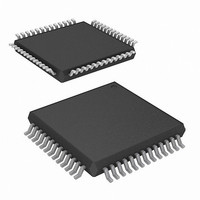
52-LQFP
Frequency-max
200MHz
Lead Free Status / RoHS Status
Lead free / RoHS Compliant
Available stocks
Company
Part Number
Manufacturer
Quantity
Price
Company:

Part Number:
CY7B9945V-2AXIT
Manufacturer:
Cypress Semiconductor Corp
Quantity:
10 000


Pin Definitions
Block Diagram Description
The PLL adjusts the phase and the frequency of its output signal
to minimize the delay between the reference (REFA/B+,
REFA/B-) and the feedback (FB) input signals.
The CY7B9945V has a flexible REF input scheme. These inputs
enable the use of either differential LVPECL or single ended
LVTTL inputs. To configure as single ended LVTTL inputs, leave
the complementary pin open (internally pulled to 1.5 V), then the
other input pin is used as a LVTTL input. The REF inputs are also
tolerant to hot insertion.
The REF inputs are changed dynamically. When changing from
one reference input to the other reference input of the same
frequency, the PLL is optimized to ensure that the clock outputs
period is not less than the calculated system budget (tMIN =
tREF (nominal reference period) – tCCJ (cycle-cycle jitter) –
tPDEV (max. period deviation)) while reacquiring lock.
The FS control pin setting determines the nominal operational
frequency range of the divide by one output (fNOM) of the
device. fNOM is directly related to the VCO frequency. The FS
setting for the device is shown in
upper fNOM range extends from 96 MHz to 200 MHz.
Table 1. Frequency Range Select
Time Unit Definition
Selectable skew is in discrete increments of time unit (t
value of a t
nominal output frequency. The equation determines the t
as follows:
t
N is a multiplication factor that is determined by the FS setting.
f
Table 2. N Factor Determination
Document Number: 38-07336 Rev. *J
25
6,9,21, 31, 45, 47 VCCN
16,27, 41
4,11,15, 23,24,
33,43,49
LOW
MID
HIGH
LOW
MID
HIGH
U
NOM
= 1/(f
FS
is nominal frequency of the device. N is defined in
FS
Pin
NOM
[1]
U
*N).
is determined by the FS setting and the maximum
32
16
N
8
MODE
VCCQ
GND
Name
Min
f
24
48
96
NOM
CY7B9945V
(MHz) at which t
Input
f
IO
NOM
Table
(MHz)
31.25
1. For CY7B9945V, the
62.5
125
Three level
Type
PWR
PWR
PWR
Input
Max
100
200
52
U
PRELIMINARY
= 1.0 ns
This pin determines the clock outputs’ disable state. When this input is
HIGH, the clock outputs disables to high impedance state (High-Z). When this
input is LOW, the clock outputs disables to HOLD-OFF mode. When in MID,
the device enters factory test mode.
Power Supply for the Output Buffers
Power Supply for the Internal Circuitry
Device Ground
Table
U
U
). The
value
2.
Divide and Phase Select Matrix
The Divide Select Matrix is comprised of three independent
banks: two of clock outputs and one for feedback. The Phase
Select Matrix, enables independent phase adjustments on
1Q[0:1], 1Q[2:3] and 2Q[0:5]. The frequency of 1Q[0:3] is
controlled by 1DS[0:1] while the frequency of 2Q[0:5] is
controlled by 2DS[0:1]. The phase of 1Q[0:1] is controlled by
1F[0:1], that of 1Q[2:3] is controlled by 1F[2:3] and that of 2Q[0:5]
is controlled by 2F[0:1].
The high fanout feedback output buffer (QF) connects to the
feedback input (FBK).This feedback output has one phase
function select input (FBF0) and two divider function selects
FBDS[0:1].
The phase capabilities that are chosen by the phase function
select pins are shown in
bank are shown in
Table 3. Output Phase Select
Table 4. Output Divider Select
and FBDS1
Control Signal
HIGH
HIGH
HIGH
[1:2]DS1
LOW
LOW
LOW
MID
MID
MID
1F1
1F3
2F1
LOW
LOW
LOW
Control Signal
FBF0
HIGH
HIGH
HIGH
LOW
LOW
LOW
1F0
1F2
2F0
MID
MID
MID
[1:2]DS0
FBDS0
HIGH
LOW
MID
and
Description
Table
1Q[0:1]
–4t
–3t
–2t
–1t
+1t
+2t
+3t
+4t
0t
Table
U
4.
U
U
U
U
U
U
U
U
Bank1
Output Phase Function
/ 1
/ 2
/ 3
Output Divider Function
3. The divide capabilities for each
1Q[2:3]
–4t
–3t
–2t
–1t
+1t
+2t
+3t
+4t
0t
U
U
U
U
U
U
U
U
U
Bank2
BK1Q[0:1]
BK1Q[2:3]
/ 1
/ 2
/ 3
RoboClock
2Q[0:5]
CY7B9945V
–8t
–7t
–6t
+6t
+7t
+8t
0t
U
U
U
U
U
U
U
Feedback
[2]
[2]
Page 4 of 15
/ 1
/ 2
/ 3
+4t
–4t
N/A
N/A
N/A
N/A
N/A
N/A
QF
0t
U
U
U
®
[+] Feedback
Related parts for CY7B9945V-2AXIT
Image
Part Number
Description
Manufacturer
Datasheet
Request
R

Part Number:
Description:
IC CLK BUFF 11OUT 200MHZ 52LQFP
Manufacturer:
Cypress Semiconductor Corp
Datasheet:
Part Number:
Description:
IC CLK BUFF 11OUT 200MHZ 52LQFP
Manufacturer:
Cypress Semiconductor Corp
Datasheet:

Part Number:
Description:
Manufacturer:
Cypress Semiconductor Corp
Datasheet:
Part Number:
Description:
Manufacturer:
Cypress Semiconductor Corp
Datasheet:
Part Number:
Description:
Manufacturer:
Cypress Semiconductor Corp
Datasheet:

Part Number:
Description:
CY7B9945V-2AXC
Manufacturer:
Cypress Semiconductor Corp
Datasheet:
Part Number:
Description:
CY7B9945V-2AXI
Manufacturer:
Cypress Semiconductor Corp
Datasheet:
Part Number:
Description:
CY7B9945V-2AXCT
Manufacturer:
Cypress Semiconductor Corp
Datasheet:
Part Number:
Description:
Manufacturer:
Cypress Semiconductor Corp
Datasheet: