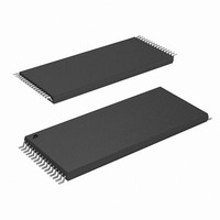
CY62128EV30LL-45ZXIT Cypress Semiconductor Corp, CY62128EV30LL-45ZXIT Datasheet - Page 9

CY62128EV30LL-45ZXIT
Manufacturer Part Number
CY62128EV30LL-45ZXIT
Description
CY62128EV30LL-45ZXIT
Manufacturer
Cypress Semiconductor Corp
Specifications of CY62128EV30LL-45ZXIT
Format - Memory
RAM
Memory Type
SRAM
Memory Size
1M (128K x 8)
Speed
45ns
Interface
Parallel
Voltage - Supply
2.2 V ~ 3.6 V
Operating Temperature
-40°C ~ 85°C
Package / Case
32-TSOP I
Density
1Mb
Access Time (max)
45ns
Sync/async
Asynchronous
Architecture
Not Required
Clock Freq (max)
Not RequiredMHz
Operating Supply Voltage (typ)
3V
Address Bus
17b
Package Type
TSOP-I
Operating Temp Range
-40C to 85C
Number Of Ports
1
Supply Current
16mA
Operating Supply Voltage (min)
2.2V
Operating Supply Voltage (max)
3.6V
Operating Temperature Classification
Industrial
Mounting
Surface Mount
Pin Count
32
Word Size
8b
Number Of Words
128K
Lead Free Status / RoHS Status
Lead free / RoHS Compliant
Lead Free Status / RoHS Status
Lead free / RoHS Compliant
Available stocks
Company
Part Number
Manufacturer
Quantity
Price
Company:
Part Number:
CY62128EV30LL-45ZXIT
Manufacturer:
CRYSTAL
Quantity:
1 408
Part Number:
CY62128EV30LL-45ZXIT
Manufacturer:
CYPRESS/赛普拉斯
Quantity:
20 000
Switching Waveforms
Notes
Document #: 38-05579 Rev. *J
24. The internal write time of the memory is defined by the overlap of WE, CE = V
25. CE is the logical combination of CE
26. Data I/O is high impedance if OE = V
27. If CE
28. During this period, the I/Os are in output state. Do not apply input signals.
ADDRESS
ADDRESS
terminate a write by going INACTIVE. The data input setup and hold timing should be referenced to the edge of the signal that terminates the write.
DATA I/O
DATA I/O
1
goes HIGH or CE
WE
WE
OE
CE
CE
NOTE 28
2
goes LOW simultaneously with WE HIGH, the output remains in high impedance state.
Figure 9. Write Cycle No. 2 (CE
1
(continued)
and CE
IH
t
SA
Figure 8. Write Cycle No. 1 (WE Controlled)
.
t
HZOE
2
. When CE
t
SA
1
is LOW and CE
t
AW
t
AW
t
SCE
2
t
t
WC
WC
is HIGH, CE is LOW; when CE
1
IL
or CE
. All signals must be ACTIVE to initiate a write and any of these signals can
t
PWE
t
t
PWE
DATA VALID
SD
2
Controlled)
t
DATA VALID
SCE
t
SD
[24, 25, 26, 27]
[24, 25, 26, 27]
1
is HIGH or CE
t
HD
t
HA
CY62128EV30 MoBL
t
HA
t
HD
2
is LOW, CE is HIGH.
Page 9 of 18
®
[+] Feedback


