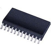
CS5460A-BSZR Cirrus Logic Inc, CS5460A-BSZR Datasheet - Page 8

CS5460A-BSZR
Manufacturer Part Number
CS5460A-BSZR
Description
IC Sngl-Phs Bi-Directional Power/Energy
Manufacturer
Cirrus Logic Inc
Datasheet
1.CS5460A-BSZ.pdf
(54 pages)
Specifications of CS5460A-BSZR
Input Impedance
30 KOhm
Measurement Error
0.1%
Voltage - I/o High
0.8V
Voltage - I/o Low
0.2V
Current - Supply
2.9mA
Voltage - Supply
4.75 V ~ 5.25 V
Operating Temperature
-40°C ~ 85°C
Mounting Type
Surface Mount
Package / Case
24-SSOP
Meter Type
Single Phase
Lead Free Status / RoHS Status
Lead free / RoHS Compliant
For Use With
CDB5460AU - EVALUATION BOARD FOR CS5460A
Lead Free Status / Rohs Status
Lead free / RoHS Compliant
Available stocks
Company
Part Number
Manufacturer
Quantity
Price
Company:
Part Number:
CS5460A-BSZR
Manufacturer:
CIRRUS
Quantity:
8 000
Part Number:
CS5460A-BSZR
Manufacturer:
CIRRUS
Quantity:
20 000
3.3 V DIGITAL CHARACTERISTICS
(T
Notes: 15. All measurements performed under static conditions.
ABSOLUTE MAXIMUM RATINGS
(DGND = 0 V; See Note 17) WARNING: Operation at or beyond these limits may result in permanent damage to
the device. Normal operation is not guaranteed at these extremes.
Notes: 17. All voltages with respect to ground.
8
High-Level Input Voltage
Low-Level Input Voltage
High-Level Output Voltage (except XIN, XOUT) I
Low-Level Output Voltage (except XIN, XOUT) I
Input Leakage Current
3-State Leakage Current
Digital Output Pin Capacitance
DC Power Supplies
Input Current, Any Pin Except Supplies(Note 20, 21, and 22)
Output Current
Power Dissipation
Analog Input Voltage
Digital Input Voltage
Ambient Operating Temperature
Storage Temperature
A
= -40 °C to +85 °C; VA+ = 5 V ±10%, VD+ = 3.3 V ±10%; VA-, DGND = 0 V) (See Notes 3, 4, and 13)
16. If VD+ = 3 V and if XIN input is generated using crystal, then XIN frequency must remain between
18. VA+ and VA- must satisfy {(VA+) - (VA-)} ≤ +6.0 V.
19. VD+ and VA- must satisfy {(VD+) - (VA-)} ≤ +6.0 V.
20. Applies to all pins including continuous over-voltage conditions at the analog input (AIN) pins.
21. Transient current of up to 100 mA will not cause SCR latch-up.
22. Maximum DC input current for a power supply pin is ±50 mA.
23. Total power dissipation, including all input currents and output currents.
2.5 MHz - 5.0 MHz. If using oscillator, full XIN frequency range is available, see Switching
Characteristics.
All Pins Except XIN, XOUT, SCLK, and RESET
All Pins Except XIN, XOUT, SCLK, and RESET
Parameter
Parameter
SCLK and RESET
SCLK and RESET
(Notes 18 and 19)
Negative Analog
Positive Analog
All Analog Pins
Positive Digital
All Digital Pins
out
out
(Note 14)
(Note 23)
= +5 mA
= -5 mA
XIN
XIN
Symbol
Symbol
V
C
V
V
V
V
I
VD+
I
V
VA+
VA-
T
I
OUT
OZ
OH
I
P
T
OL
out
in
IND
IH
INA
IL
IN
stg
A
D
(VD+) - 0.5
(VD+) - 1.0
DGND - 0.3
(VA-) - 0.3
0.6 VD+
0.8 VD+
Min
+0.3
Min
-0.3
-0.3
-40
-65
-
-
-
-
-
-
-
-
-
-
Typ
Typ
±1
5
-
-
-
-
-
-
-
-
-
-
-
-
-
-
-
-
-
-
-
(VD+) + 0.3
(VA+) + 0.3
0.2 VD+
Max
0.48
±10
±10
Max
+6.0
+6.0
0.3
0.4
-6.0
±10
±25
500
150
CS5460A
85
-
-
-
-
-
DS487F4
Unit
Unit
µA
µA
mW
pF
mA
mA
V
V
V
V
V
V
V
V
°C
°C
V
V
V
V
V


