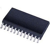
CS5460A-BSZR Cirrus Logic Inc, CS5460A-BSZR Datasheet - Page 30

CS5460A-BSZR
Manufacturer Part Number
CS5460A-BSZR
Description
IC Sngl-Phs Bi-Directional Power/Energy
Manufacturer
Cirrus Logic Inc
Datasheet
1.CS5460A-BSZ.pdf
(54 pages)
Specifications of CS5460A-BSZR
Input Impedance
30 KOhm
Measurement Error
0.1%
Voltage - I/o High
0.8V
Voltage - I/o Low
0.2V
Current - Supply
2.9mA
Voltage - Supply
4.75 V ~ 5.25 V
Operating Temperature
-40°C ~ 85°C
Mounting Type
Surface Mount
Package / Case
24-SSOP
Meter Type
Single Phase
Lead Free Status / RoHS Status
Lead free / RoHS Compliant
For Use With
CDB5460AU - EVALUATION BOARD FOR CS5460A
Lead Free Status / Rohs Status
Lead free / RoHS Compliant
Available stocks
Company
Part Number
Manufacturer
Quantity
Price
Company:
Part Number:
CS5460A-BSZR
Manufacturer:
CIRRUS
Quantity:
8 000
Part Number:
CS5460A-BSZR
Manufacturer:
CIRRUS
Quantity:
20 000
pins of the voltage/current channels to their ground
reference level. (See Figure 17.)
Offset and gain calibration cannot be done at the
same time. This will cause undesirable calibration
results.
3.8.7 Description of Calibration Algo-
rithms
The computational flow of the CS5460A’s AC and
DC gain/offset calibration sequences are illustrat-
ed in Figure 18. This figure applies to both the volt-
age channel and the current channel. The
30
(DC or AC)
Full Scale
In
CM + -
0V + -
CM + -
External
Connections
Figure 17. System Calibration of Offset.
Figure 16. System Calibration of Gain.
+
-
External
Connections
M odulator
AIN+
AIN-
AIN+
AIN-
Filter
+
-
XGAIN
+
-
* Denotes readable/writable register
D C O ffse t*
XGAIN
-X
+
+
+
Figure 18. Calibration Data Flow
G a in *
x
1
x
+
-
+
-
Σ
÷
N
N
to V *, I*, P *, E * R egisters
X
2
following descriptions of calibration sequences will
focus on the voltage channel, but apply equally to
the current channel.
Note: For proper calibration, it is assumed that the value
3.8.7.1 AC Offset Calibration Sequence
The idea of the AC offset calibration is to obtain an
offset value that reflects the square of the RMS
output level when the inputs are grounded. During
normal operation, when the CS5460A is calculat-
ing the latest result for the RMS Voltage Register,
this AC offset register value will be subtracted from
the square of each successive voltage sample in
order to nullify the AC offset that may be inherent
in the voltage-channel signal path. Note that the
value in the AC offset register is proportional to the
square of the AC offset.
First, the inputs are grounded, and then the AC off-
set calibration command is sent to the CS5460A.
When the AC offset calibration sequence is initiat-
ed, a valid RMS Voltage Register value is acquired
and squared. This value is then subtracted from
the square of each voltage sample that comes
through the RMS data path. See Figure 18.
A C O ffse t*
+
+
-
of the Voltage-/Current-Channel Gain Registers
are set to default (1.0) before running the gain
calibration(s),
Voltage-/Current Channel AC and DC Offset
Registers is set to default (0) before running
calibrations.
software or hardware reset of the device. The
values in the voltage/current calibration registers
do affect the results of the calibration sequences.
S IN C
2
X
0 .6
x
2
N
This can be accomplished by a
and
X
the
÷
N
value
CS5460A
DS487F4
V R M S
in
*
the


