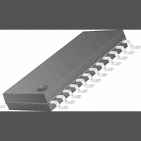
CS43L42-KZ Cirrus Logic Inc, CS43L42-KZ Datasheet - Page 26

CS43L42-KZ
Manufacturer Part Number
CS43L42-KZ
Description
D/A Converter (D-A) IC
Manufacturer
Cirrus Logic Inc
Specifications of CS43L42-KZ
No. Of Pins
24
Peak Reflow Compatible (260 C)
No
No. Of Bits
24 Bit
Leaded Process Compatible
No
Mounting Type
Surface Mount
Interface Type
Serial
Package / Case
24-TSSOP
Lead Free Status / RoHS Status
Contains lead / RoHS non-compliant
Available stocks
Company
Part Number
Manufacturer
Quantity
Price
Part Number:
CS43L42-KZ
Manufacturer:
CIRRUS
Quantity:
20 000
Company:
Part Number:
CS43L42-KZZ
Manufacturer:
CIRRUS
Quantity:
148
Part Number:
CS43L42-KZZ
Manufacturer:
CIRRUSLOGIC
Quantity:
20 000
LRCK
SDATA
AD0/CS
(Control Port Mode)
SCLK
RST
5. PIN DESCRIPTION
26
HP Quiescent Voltage
Serial Clock/DEM1
SCL/CCLK/DIF1
SDA/CDIN/DIF0
Left/Right Clock
Interface Power
AD0/CS/DEM0
No Connection
Master Clock
Mode Select
Serial Data
Reset
1
2
3
4
5
SCL/CCLK/DIF1
SDA/CDIN/DIF0
AD0/CS/DEM0
Reset (Input) - The device enters a low power mode and all internal registers are reset to
their default settings, including the control port, when low. When high, the control port
becomes operational and the PDN bit must be cleared before normal operation will occur.
The control port cannot be accessed when Reset is low.
Left/Right Clock (Input) - Determines which channel is currently being input on the serial
audio data input, SDATA. The frequency of the Left/Right clock must be equal to the input
sample rate. Audio samples in Left/Right sample pairs will be simultaneously output from
the digital-to-analog converter whereas Right/Left pairs will exhibit a one sample period dif-
ference. The required relationship between the Left/Right clock, serial clock and serial data
is defined by the Mode Control 2 (0Bh) register when in Control Port Mode or by the DIF1-0
pins when in Stand-Alone mode. The options are detailed in Figures 19-29.
Serial Audio Data (Input) - Two's complement MSB-first serial data is input on this pin. The
data is clocked into SDATA via the serial clock and the channel is determined by the
Left/Right clock. The required relationship between the Left/Right clock, serial clock and
serial data is defined by the Mode Control 2 (0Bh) register when in Control Port Mode or by
the DIF1-0 pins when in Stand-Alone mode. The options are detailed in Figures 19-29.
Address Bit / Chip Select (Input) - In Two-Wire mode, AD0 is a chip address bit. CS is
used to enable the control port interface in SPI mode. The device will enter the SPI mode
anytime a high to low transition is detected on this pin. Once the device has entered the
SPI mode, it will remain in SPI mode until either the part is reset or power is removed.
Serial Clock (Input) - Clocks the individual bits of the serial data into the SDATA pin. The
required relationship between the Left/Right clock, serial clock and serial data is defined by
the Mode Control 2 (0Bh) register when in Control Port Mode or by the DIF1-0 pins when in
Stand-Alone mode. The options are detailed in Figures 19-29.
The CS43L42 supports both internal and external serial clock generation modes. The Inter-
nal Serial Clock Mode eliminates possible clock interference from an external SCLK. Use
of the Internal Serial Clock Mode is always preferred.
Internal Serial Clock Mode - In the Internal Serial Clock Mode, the serial clock is internally
derived and synchronous with the master clock and left/right clock. The SCLK/LRCK fre-
quency ratio is either 32, 48, or 64 depending upon the Mode Control 2 (0Bh) register when
in Control Port Mode or the DIF1-0 pins when in Stand-Alone mode as shown in Figures
19-29. Operation in this mode is identical to operation with an external serial clock synchro-
nized with LRCK.
External Serial Clock Mode - The CS43L42 will enter the External Serial Clock Mode when-
ever 16 low to high transitions are detected on the SCLK pin during any phase of the LRCK
period. The device will revert to Internal Serial Clock Mode if no low to high transitions are
detected on the SCLK pin for 2 consecutive periods of LRCK.
SCLK/DEM1
SDATA
VQ_HP
CP/SA
MCLK
LRCK
RST
N.C.
VL
1
1
2
2
3
4
5
5
6
6
7
8
9
10
11
12
24
23
22
21
20
19
18
17
16
15
14
13
MUTEC
AOUTA
AOUTB
HP_B
VA_HP
VA_LINE
VA
GND
HP_A
VQ_LINE
FILT+
REF_GND
Mute Control
Analog Output A
Analog Output B
Headphone Output B
Headphone Amp Power
Line Amp Power
Analog Power
Ground
Headphone Output A
Line Out Quiescent Voltage
Positive Voltage Reference
Reference Ground
CS43L42
DS481PP2


