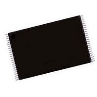
AM29F200BB-90EC Spansion Inc., AM29F200BB-90EC Datasheet - Page 15

AM29F200BB-90EC
Manufacturer Part Number
AM29F200BB-90EC
Description
Flash Memory IC
Manufacturer
Spansion Inc.
Datasheets
1.AM29F200BT-90EI.pdf
(41 pages)
2.AM29F200BT-90EI.pdf
(41 pages)
3.AM29F200BT-90EI.pdf
(41 pages)
4.AM29F200BB-90EC.pdf
(42 pages)
Specifications of AM29F200BB-90EC
Memory Size
2Mbit
Memory Configuration
256K X 8
Ic Interface Type
Parallel
Access Time
90ns
Memory Case Style
TSOP
No. Of Pins
48
Operating Temperature Range
0°C To +70°C
Termination Type
SMD
Lead Free Status / RoHS Status
Contains lead / RoHS non-compliant
Available stocks
Company
Part Number
Manufacturer
Quantity
Price
Company:
Part Number:
AM29F200BB-90EC
Manufacturer:
AMD
Quantity:
6 100
Company:
Part Number:
AM29F200BB-90EC
Manufacturer:
SPANSION
Quantity:
399
Part Number:
AM29F200BB-90EC
Manufacturer:
AMD
Quantity:
20 000
Method) table, which is intended for PROM program-
mers and requires V
The autoselect command sequence is initiated by
writing two unlock cycles, followed by the autoselect
command. The device then enters the autoselect
mode, and the system may read at any address any
number of times, without initiating another command
sequence.
A read cycle at address XX00h retrieves the manufac-
turer code. A read cycle at address XX01h in word
mode (or 02h in byte mode) returns the device code. A
read cycle containing a sector address (SA) and the
address 02h in word mode (or 04h in byte mode)
returns 01h if that sector is protected, or 00h if it is
unprotected. Refer to the Sector Address tables for
valid sector addresses.
The system must write the reset command to exit the
autoselect mode and return to reading array data.
Word/Byte Program Command Sequence
The system may program the device by byte or word,
on depending on the state of the BYTE# pin. Program-
ming is a four-bus-cycle operation. The program
command sequence is initiated by writing two unlock
write cycles, followed by the program set-up command.
The program address and data are written next, which
in turn initiate the Embedded Program algorithm. The
system is not required to provide further controls or tim-
ings. The device automatically provides internally
generated program pulses and verify the programmed
cell margin. The Command Definitions take shows the
address and data requirements for the byte program
command sequence.
When the Embedded Program algorithm is complete,
the device then returns to reading array data and
addresses are no longer latched. The system can
determine the status of the program operation by using
DQ7, DQ6, or RY/BY#. See “Write Operation Status”
for information on these status bits.
Any commands written to the device during the
Embedded Program Algorithm are ignored. Note that a
hardware reset immediately terminates the program-
ming operation. The program command sequence
should be reinitiated once the device has reset to
reading array data, to ensure data integrity.
Programming is allowed in any sequence and across
sector boundaries. A bit cannot be programmed
from a “0” back to a “1”. Attempting to do so may halt
the operation and set DQ5 to “1”, or cause the Data#
Polling algorithm to indicate the operation was suc-
cessful. However, a succeeding read will show that the
data is still “0”. Only erase operations can convert a “0”
to a “1”.
November 1, 2006 21526D4
ID
on address bit A9.
D A T A
Am29F200B
S H E E T
Note: See the appropriate Command Definitions table for
program command sequence.
Chip Erase Command Sequence
Chip erase is a six-bus-cycle operation. The chip erase
command sequence is initiated by writing two unlock
cycles, followed by a set-up command. Two additional
unlock write cycles are then followed by the chip erase
command, which in turn invokes the Embedded Erase
algorithm. The device does not require the system to
preprogram prior to erase. The Embedded Erase algo-
rithm automatically preprograms and verifies the entire
memory for an all zero data pattern prior to electrical
erase. The system is not required to provide any con-
trols or timings during these operations. The Command
Definitions table shows the address and data require-
ments for the chip erase command sequence.
Any commands wr itten to the chip dur ing the
Embedded Erase algorithm are ignored. Note that a
hardware reset during the chip erase operation imme-
diately terminates the operation. The Chip Erase
command sequence should be reinitiated once the
device has returned to reading array data, to ensure
data integrity.
Increment Address
Figure 2. Program Operation
in progress
Embedded
algorithm
Program
No
Command Sequence
Write Program
Last Address?
Programming
from System
Verify Data?
Completed
Data Poll
START
Yes
Yes
No
13


