ADXL345BCCZ-RL Analog Devices Inc, ADXL345BCCZ-RL Datasheet - Page 25
ADXL345BCCZ-RL
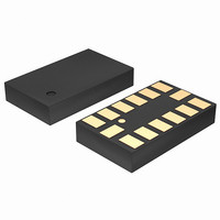
Manufacturer Part Number
ADXL345BCCZ-RL
Description
Digital Output Three-Axis Accel 4K RL
Manufacturer
Analog Devices Inc
Series
iMEMS®r
Datasheet
1.EVAL-ADXL345Z.pdf
(40 pages)
Specifications of ADXL345BCCZ-RL
Design Resources
Sensing Low-g Acceleration Using ADXL345 Digital Accelerometer Connected to ADuC7024 (CN0133)
Axis
X, Y, Z
Acceleration Range
±2g, 4g, 8g, 16g
Sensitivity
256LSB/g, 128LSB/g, 64LSB/g, 32LSB/g
Voltage - Supply
2 V ~ 3.6 V
Output Type
Digital
Bandwidth
6.25Hz ~ 3.2kHz Selectable
Interface
I²C, SPI
Mounting Type
Surface Mount
Package / Case
14-LGA
Package Type
LGA
Operating Supply Voltage (typ)
2.5V
Operating Supply Voltage (max)
3.6V
Operating Temperature (min)
-40C
Operating Temperature (max)
85C
Operating Temperature Classification
Industrial
Product Depth (mm)
3mm
Product Length (mm)
5mm
Mounting
Surface Mount
Pin Count
14
Lead Free Status / RoHS Status
Lead free / RoHS Compliant
Lead Free Status / RoHS Status
Lead free / RoHS Compliant
Other names
ADXL345BCCZ-RLTR
Available stocks
Company
Part Number
Manufacturer
Quantity
Price
Company:

Part Number:
ADXL345BCCZ-RL7
Manufacturer:
POWER
Quantity:
14 300


ACT_x Enable Bits and INACT_x Enable Bits
A setting of 1 enables x-, y-, or z-axis participation in detecting
activity or inactivity. A setting of 0 excludes the selected axis from
participation. If all axes are excluded, the function is disabled.
For activity detection, all participating axes are logically OR’ e d,
causing the activity function to trigger when any of the partici-
pating axes exceeds the threshold. For inactivity detection, all
participating axes are logically AND’ e d, causing the inactivity
function to trigger only if all participating axes are below the
threshold for the specified time.
Register 0x28—THRESH_FF (Read/Write)
The THRESH_FF register is eight bits and holds the threshold
value, in unsigned format, for free-fall detection. The acceleration on
all axes is compared with the value in THRESH_FF to determine if
a free-fall event occurred. The scale factor is 62.5 mg/LSB. Note
that a value of 0 mg may result in undesirable behavior if the free-
fall interrupt is enabled. Values between 300 mg and 600 mg
(0x05 to 0x09) are recommended.
Register 0x29—TIME_FF (Read/Write)
The TIME_FF register is eight bits and stores an unsigned time
value representing the minimum time that the value of all axes
must be less than THRESH_FF to generate a free-fall interrupt.
The scale factor is 5 ms/LSB. A value of 0 may result in undesirable
behavior if the free-fall interrupt is enabled. Values between 100 ms
and 350 ms (0x14 to 0x46) are recommended.
Register 0x2A—TAP_AXES (Read/Write)
D7
0
Suppress Bit
Setting the suppress bit suppresses double tap detection if
acceleration greater than the value in THRESH_TAP is present
between taps. See the Tap Detection section for more details.
TAP_x Enable Bits
A setting of 1 in the TAP_X enable, TAP_Y enable, or TAP_Z
enable bit enables x-, y-, or z-axis participation in tap detection.
A setting of 0 excludes the selected axis from participation in
tap detection.
Register 0x2B—ACT_TAP_STATUS (Read Only)
D7
0
ACT_x Source and TAP_x Source Bits
These bits indicate the first axis involved in a tap or activity
event. A setting of 1 corresponds to involvement in the event,
and a setting of 0 corresponds to no involvement. When new
data is available, these bits are not cleared but are overwritten by
the new data. The ACT_TAP_STATUS register should be read
before clearing the interrupt. Disabling an axis from participation
clears the corresponding source bit when the next activity or
single tap/double tap event occurs.
D6
ACT_X
source
D6
0
D5
ACT_Y
source
D5
0
D4
0
D4
ACT_Z
source
D3
Suppress
D3
Asleep
D2
TAP_X
enable
D2
TAP_X
source
D1
TAP_Y
enable
D1
TAP_Y
source
D0
TAP_Z
enable
D0
TAP_Z
source
Rev. B | Page 25 of 40
Asleep Bit
A setting of 1 in the asleep bit indicates that the part is asleep,
and a setting of 0 indicates that the part is not asleep. This bit
toggles only if the device is configured for auto sleep. See the
AUTO_SLEEP Bit section for more information on autosleep
mode.
Register 0x2C—BW_RATE (Read/Write)
D7
0
LOW_POWER Bit
A setting of 0 in the LOW_POWER bit selects normal operation,
and a setting of 1 selects reduced power operation, which has
somewhat higher noise (see the Power Modes section for details).
Rate Bits
These bits select the device bandwidth and output data rate (see
Table 7 and Table 8 for details). The default value is 0x0A, which
translates to a 100 Hz output data rate. An output data rate should
be selected that is appropriate for the communication protocol
and frequency selected. Selecting too high of an output data rate with
a low communication speed results in samples being discarded.
Register 0x2D—POWER_CTL (Read/Write)
D7
0
Link Bit
A setting of 1 in the link bit with both the activity and inactivity
functions enabled delays the start of the activity function until
inactivity is detected. After activity is detected, inactivity detection
begins, preventing the detection of activity. This bit serially links
the activity and inactivity functions. When this bit is set to 0,
the inactivity and activity functions are concurrent. Additional
information can be found in the Link Mode section.
When clearing the link bit, it is recommended that the part be
placed into standby mode and then set back to measurement
mode with a subsequent write. This is done to ensure that the
device is properly biased if sleep mode is manually disabled;
otherwise, the first few samples of data after the link bit is cleared
may have additional noise, especially if the device was asleep
when the bit was cleared.
AUTO_SLEEP Bit
If the link bit is set, a setting of 1 in the AUTO_SLEEP bit enables
the auto-sleep functionality. In this mode, the ADXL345 auto-
matically switches to sleep mode if the inactivity function is
enabled and inactivity is detected (that is, when acceleration is
below the THRESH_INACT value for at least the time indicated
by TIME_INACT). If activity is also enabled, the ADXL345
automatically wakes up from sleep after detecting activity and
returns to operation at the output data rate set in the BW_RATE
register. A setting of 0 in the AUTO_SLEEP bit disables automatic
switching to sleep mode. See the description of the Sleep Bit in
this section for more information on sleep mode.
D6
0
D6
0
D5
Link
D5
0
D4
AUTO_SLEEP
D4
LOW_POWER
D3
Measure
D3
D2
D2
Sleep
Rate
ADXL345
D1
D1
Wakeup
D0
D0
Related parts for ADXL345BCCZ-RL
Image
Part Number
Description
Manufacturer
Datasheet
Request
R

Part Number:
Description:
±1.7g Dual-Axis IMEMS Accelerometer Evaluation Board
Manufacturer:
Analog Devices Inc
Datasheet:

Part Number:
Description:
Inertial Sensor Evaluation System
Manufacturer:
Analog Devices Inc
Datasheet:
Part Number:
Description:
Manufacturer:
Analog Devices Inc
Datasheet:
Part Number:
Description:
Manufacturer:
Analog Devices Inc
Datasheet:
Part Number:
Description:
Manufacturer:
Analog Devices Inc
Datasheet:
Part Number:
Description:
Manufacturer:
Analog Devices Inc
Datasheet:
Part Number:
Description:
Manufacturer:
Analog Devices Inc
Datasheet:
Part Number:
Description:
Manufacturer:
Analog Devices Inc
Datasheet:
Part Number:
Description:
Manufacturer:
Analog Devices Inc
Datasheet:
Part Number:
Description:
Manufacturer:
Analog Devices Inc
Datasheet:
Part Number:
Description:
Manufacturer:
Analog Devices Inc
Datasheet:
Part Number:
Description:
Manufacturer:
Analog Devices Inc
Datasheet:
Part Number:
Description:
Manufacturer:
Analog Devices Inc
Datasheet: