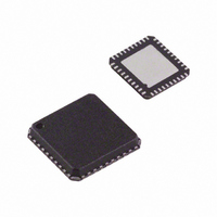
ADV7179KCP Analog Devices Inc, ADV7179KCP Datasheet - Page 21

ADV7179KCP
Manufacturer Part Number
ADV7179KCP
Description
IC,TV/VIDEO CIRCUIT,Video Encoder,LLCC,40PIN,CERAMIC
Manufacturer
Analog Devices Inc
Type
Video Encoderr
Datasheet
1.ADV7179KCPZ.pdf
(52 pages)
Specifications of ADV7179KCP
Rohs Status
RoHS non-compliant
Applications
Digital Cameras, Mobile Phones, Portable Video
Voltage - Supply, Analog
2.8 V, 3.3 V
Mounting Type
Surface Mount
Package / Case
40-LFCSP
Voltage - Supply, Digital
-
Lead Free Status / RoHS Status
Available stocks
Company
Part Number
Manufacturer
Quantity
Price
Company:
Part Number:
ADV7179KCP
Manufacturer:
AD
Quantity:
1 303
Company:
Part Number:
ADV7179KCP
Manufacturer:
ADI
Quantity:
244
Company:
Part Number:
ADV7179KCPZ
Manufacturer:
ADI
Quantity:
250
Part Number:
ADV7179KCPZ
Manufacturer:
ADI/亚德诺
Quantity:
20 000
Company:
Part Number:
ADV7179KCPZ-REE1
Manufacturer:
SARC
Quantity:
92
Company:
Part Number:
ADV7179KCPZ-REEL
Manufacturer:
TI
Quantity:
69 456
Part Number:
ADV7179KCPZ-REEL
Manufacturer:
ADI/亚德诺
Quantity:
20 000
Mode 1: Master Option HSYNC , BLANK , FIELD
(Timing Register 0 TR0 = X X X X X 0 1 1)
In this mode, the ADV7174/ADV7179 can generate horizontal
SYNC and odd/even FIELD signals. A transition of the FIELD
input when HSYNC is low indicates a new frame, i.e., vertical
retrace. The BLANK signal is optional. When the BLANK input
HSYNC
BLANK
FIELD
PIXEL
DATA
NTSC = 16 × CLOCK/2
PAL = 12 × CLOCK/2
Figure 26. Timing Mode 1 Odd/Even Field Transitions Master/Slave
Rev. B | Page 21 of 52
is disabled, the ADV7174/ADV7179 automatically blanks all
normally blank lines as per CCIR-624. Pixel data is latched on
the rising clock edge following the timing signal transitions.
Mode 1 is illustrated in
Figure 26
odd or even field transition relative to the pixel data.
illustrates the
PAL = 132 × CLOCK/2
NTSC = 122 × CLOCK/2
Figure 24
Cb
HSYNC , BLANK , and FIELD for an
Y
Cr
(NTSC) and
ADV7174/ADV7179
Y
Figure 25
(PAL).


