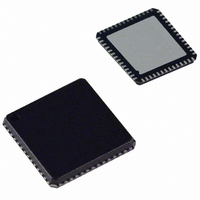
ADUC842BCPZ62-3 Analog Devices Inc, ADUC842BCPZ62-3 Datasheet - Page 38

ADUC842BCPZ62-3
Manufacturer Part Number
ADUC842BCPZ62-3
Description
Microconverter 1-cycle Version ADUC832
Manufacturer
Analog Devices Inc
Series
MicroConverter® ADuC8xxr
Specifications of ADUC842BCPZ62-3
Core Processor
8052
Core Size
8-Bit
Speed
8.38MHz
Connectivity
I²C, SPI, UART/USART
Peripherals
DMA, PSM, PWM, Temp Sensor, WDT
Number Of I /o
32
Program Memory Size
62KB (62K x 8)
Program Memory Type
FLASH
Ram Size
2.25K x 8
Voltage - Supply (vcc/vdd)
2.7 V ~ 3.6 V
Data Converters
A/D 8x12b, D/A 2x12b
Oscillator Type
Internal
Operating Temperature
-40°C ~ 85°C
Package / Case
56-LFCSP
Lead Free Status / RoHS Status
Lead free / RoHS Compliant
Eeprom Size
-
Lead Free Status / RoHS Status
Lead free / RoHS Compliant
Bit No.
7
6
5
4
3
2
1
0
ADuC841/ADuC842/ADuC843
USER INTERFACE TO ON-CHIP PERIPHERALS
This section gives a brief overview of the various peripherals
also available on-chip. A summary of the SFRs used to control
and configure these peripherals is also given.
DAC
The ADuC841/ADuC842 incorporate two 12-bit voltage output
DACs on-chip. Each has a rail-to-rail voltage output buffer
capable of driving 10 kΩ/100 pF. Each has two selectable ranges,
0 V to V
AV
Table 15. DACCON SFR Bit Designations
DACxH/L
Function
SFR Address
Power-On Default
Bit Addressable
The 12-bit DAC data should be written into DACxH/L right-justified such that DACxL contains the lower 8 bits, and the lower nibble of
DACxH contains the upper 4 bits.
DD
. Each can operate in 12-bit or 8-bit mode.
REF
Name
MODE
RNG1
RNG0
CLR1
CLR0
SYNC
PD1
PD0
(the internal band gap 2.5 V reference) and 0 V to
Description
The DAC MODE bit sets the overriding operating mode for both DACs.
Set to 1 by the user to select 8-bit mode (write 8 bits to DACxL SFR).
Set to 0 by the user to select 12-bit mode.
DAC1 Range Select Bit.
Set to 1 by the user to select the range for DAC1 as 0 V to V
Set to 0 by the user to select the range for DAC1 as 0 V to V
DAC0 Range Select Bit.
Set to 1 by the user to select the range for DAC0 as 0 V to V
Set to 0 by the user to select the range for DAC0 as 0 V to V
DAC1 Clear Bit.
Set to 1 by the user to leave the output of DAC1 at its normal level.
Set to 0 by the user to force the output of DAC1 to 0 V.
DAC0 Clear Bit.
Set to 1 by the user to leave the output of DAC0 at its normal level.
Set to 0 by the user to force the output of DAC0 to 0 V.
DAC0/1 Update Synchronization Bit.
When set to 1, the DAC outputs update as soon as DACxL SFRs are written. The user can simultaneously update
both DACs by first updating the DACxL/H SFRs while SYNC is 0. Both DACs then update simultaneously when the
SYNC bit is set to 1.
DAC1 Power-Down Bit.
Set to 1 by the user to power on DAC1.
Set to 0 by the user to power off DAC1.
DAC0 Power-Down Bit.
Set to 1 by the user to power on DAC0.
Set to 0 by the user to power off DAC0.
DAC Data Registers
DAC data registers, written by the user to update the DAC output.
DAC0L (DAC0 Data Low Byte) -> F9H; DAC1L (DAC1 Data Low Byte) -> FBH
DACH (DAC0 Data High Byte) -> FAH; DAC1H (DAC1 Data High Byte) -> FCH
00H
No
All Four Registers.
All Four Registers.
Rev. 0 | Page 38 of 88
Both DACs share a control register, DACCON, and four data
registers, DAC1H/L, DAC0/L. Note that in 12-bit asynchronous
mode, the DAC voltage output is updated as soon as the DACL
data SFR has been written; therefore, the DAC data registers
should be updated as DACH first, followed by DACL. Note that
for correct DAC operation on the 0 V to V
must be switched on. This results in the DAC using the correct
reference value.
DACCON
SFR Address
Power-On Default
Bit Addressable
DD
REF
DD
REF
.
.
.
.
DAC Control Register
FDH
04H
No
REF
range, the ADC


