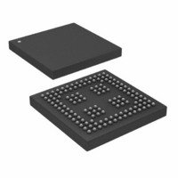
ADSP-21261SKBC-150 Analog Devices Inc, ADSP-21261SKBC-150 Datasheet - Page 7

ADSP-21261SKBC-150
Manufacturer Part Number
ADSP-21261SKBC-150
Description
150 MHz, 32Bit DSP Processor.
Manufacturer
Analog Devices Inc
Series
SHARC®r
Type
Fixed/Floating Pointr
Datasheet
1.ADSP-21261SKBCZ150.pdf
(44 pages)
Specifications of ADSP-21261SKBC-150
Interface
DAI, SPI
Clock Rate
150MHz
Non-volatile Memory
ROM (384 kB)
On-chip Ram
128kB
Voltage - I/o
3.30V
Voltage - Core
1.20V
Operating Temperature
0°C ~ 70°C
Mounting Type
Surface Mount
Package / Case
136-CSPBGA
Lead Free Status / RoHS Status
Contains lead / RoHS non-compliant
Available stocks
Company
Part Number
Manufacturer
Quantity
Price
Company:
Part Number:
ADSP-21261SKBC-150
Manufacturer:
AD
Quantity:
30
Serial Peripheral (Compatible) Interface
Serial peripheral interface is an industry-standard synchronous
serial link, enabling the ADSP-21261 SPI-compatible port to
communicate with other SPI-compatible devices. SPI is an
interface consisting of two data pins, one device select pin, and
one clock pin. It is a full-duplex synchronous serial interface,
supporting both master and slave modes. The SPI port can
operate in a multimaster environment by interfacing with up to
four other SPI-compatible devices, either acting as a master or
slave device. The ADSP-21261 SPI-compatible peripheral
implementation also features programmable baud rates up to
0x0007 8000–0x0007 DFFF
0x0007 E000–0x0007 FFFF
BLOCK 1 ROM (1.5M BIT)
0x0000 0000–0x0003 FFFF
0x0004 2000–0x0005 7FFF
0x0005 8000–0x0002 FFFF
BLOCK 0 SRAM (0.5M B IT)
BLOCK 0 R OM (1.5M B IT)
0x0005 3000–0x0005 FFFF
BLOCK 1 SRAM (0.5M B IT)
0x0006 2000–0x0007 7FFF
0x0004 0000–0x0004 1FFF
0x0006 0000–0x0006 1FFF
ADDRESSING
LONG WORD
IOP REGISTERS
RESERVED
RESERVED
RESERVED
RESERVED
0x000B C000–0x000B FFFF
0x000B 0000–0x000B BFFF
BLOCK 0 ROM (1.5M BIT) 2
0x0008 4000 - 0x000A FFFF
0x0300 0000–0x3FFF FFFF
BLOCK 1 SRAM (0.5M B IT)
0x000C 0000–0x000C 3FFF
0x000F C000–0x000F FFFF
BLOCK 0 SRAM ( 0.5M BIT)
EXTERNAL MEMORY
Figure 3. ADSP-21261 Memory Map
0x000C 4000–0x000E FFFF
BLOCK 1 ROM (1.5M BIT) 3
0x000F 0000–0x000F BFFF
0x0000 0000–0x0003 FFFF
0x0008 0000–0x0008 3FFF
0x0020 0000–0x00FF FFFF
0x0100 0000–0x02FF FFFF
INTERNAL MEMORY
Rev. 0 | Page 7 of 44 | March 2006
NORMAL WORD
ADDRESS SPACE 1
ADDRESSING
IOP REGISTERS
EXTERN AL DMA
RESERVED
RESERVED
RESERVED
RESERVED
RESERVED
RESERVED
SPACE
SPACE
37.5 MHz, clock phases, and polarities. The ADSP-21261 SPI-
compatible port uses open-drain drivers to support a multimas-
ter configuration and to avoid data contention.
Parallel Port
The parallel port provides interfaces to SRAM and peripheral
devices. The multiplexed address and data pins (AD15–0) can
access 8-bit devices with up to 24 bits of address, or 16-bit
devices with up to 16 bits of address. In either mode, 8- or 16-
bit, the maximum data transfer rate is one-third the core clock
speed. As an example, a clock rate of 200 MHz is equivalent to
66M byte/s, and a clock rate of 150 MHz is equivalent to
50M byte/s.
1 EXTERNAL MEMORY IS NOT DIRECTLY
2 B LOC K 0 ROM HA S A 48-BIT ADDRESS RA NGE
3 B LOC K 1 ROM HA S A 48-BIT ADDRESS RA NGE
A CCESSIBLE BY THE CORE. DMA MUST BE
U SED TO READ OR WRITE TO THIS MEM O R Y
( 0xA0000–0xA7 FFFF).
( 0xE0000–0xE7 FFFF).
U S I N G T H E S P I O R P A R A L L E L P O R T .
0x0017 8FFF–0x0017 FFFF
0x001E 0000–0x001F 7FFF
BLOCK 1 ROM ( 1.5M BIT)
0x0018 8000–0x001D FFFF
0x0016 0000–0x0017 7FFF
B LOCK 0 SRAM (0.5M BIT)
0x0010 8000–0x0015 FFFF
BLOCK 0 ROM (1.5M BIT)
B LOCK 1 SRAM (0.5M BIT)
0x0000 0000–0x0003 FFFF
0x0010 0000–0x0010 7FFF
0x0018 0000–0x0018 7FFF
SHORT WORD
ADDRESSING
IOP REGISTERS
RESERVED
RESERVED
R ESERVED
R ESERVED
0x000
ADSP-21261


