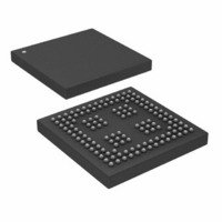
ADSP-21261SKBC-150 Analog Devices Inc, ADSP-21261SKBC-150 Datasheet - Page 37

ADSP-21261SKBC-150
Manufacturer Part Number
ADSP-21261SKBC-150
Description
150 MHz, 32Bit DSP Processor.
Manufacturer
Analog Devices Inc
Series
SHARC®r
Type
Fixed/Floating Pointr
Datasheet
1.ADSP-21261SKBCZ150.pdf
(44 pages)
Specifications of ADSP-21261SKBC-150
Interface
DAI, SPI
Clock Rate
150MHz
Non-volatile Memory
ROM (384 kB)
On-chip Ram
128kB
Voltage - I/o
3.30V
Voltage - Core
1.20V
Operating Temperature
0°C ~ 70°C
Mounting Type
Surface Mount
Package / Case
136-CSPBGA
Lead Free Status / RoHS Status
Contains lead / RoHS non-compliant
Available stocks
Company
Part Number
Manufacturer
Quantity
Price
Company:
Part Number:
ADSP-21261SKBC-150
Manufacturer:
AD
Quantity:
30
OUTPUT DRIVE CURRENTS
Figure 28
ers of the ADSP-21261. The curves represent the current drive
capability of the output drivers as a function of output voltage.
TEST CONDITIONS
The ac signal specifications (timing parameters) appear in
Table 9 on Page 18
output disable time, output enable time, and capacitive loading.
Timing is measured on signals when they cross the 1.5 V level as
described in
sured between the point that the first signal reaches 1.5 V and
the point that the second signal reaches 1.5 V.
–20
–30
–40
–10
Figure 29. Equivalent Device Loading for AC Measurements
40
30
20
10
OUTPUT 1.5V
Figure 30. Voltage Reference Levels for AC Measurements
OUTPUT
0
0
shows typical I-V characteristics for the output driv-
INPUT
Figure
OR
PIN
TO
V OL
0.5
Figure 28. ADSP-21261 Typical Drive
through
30. All delays (in nanoseconds) are mea-
3.47V, 0°C
SWEEP (V
1.0
(Includes All Fixtures)
3.3V, 25°C
Table 31 on Page
3.11V, 70°C
1.5
DDEXT
30pF
) VOLTAGE (V)
V OH
2
3.11V, 70°C
50
3.47V, 0°C
2.5
3.3V, 25°C
36. These include
3.0
Rev. 0 | Page 37 of 44 | March 2006
1.5V
1.5V
3.5
CAPACITIVE LOADING
Output delays and holds are based on standard capacitive loads:
30 pF on all pins (see
how output delays and holds vary with load capacitance. The
graphs of
outside the ranges shown for Typical Output Delay vs. Load
Capacitance and Typical Output Rise Time (20%–80%, V =
Min) vs. Load Capacitance.
12
10
8
6
4
2
0
12
10
Figure
8
6
4
2
0
0
0
Figure 31. Typical Output Rise/Fall Time
Figure 32. Typical Output Rise/Fall Time
31,
y = 0.0904x + 1.9426
20
20
Figure
y = 0.0915x + 2.2207
(20% to 80%, V
(20% to 80%, V
Figure
LOAD CAPACITANCE (pF)
LOAD CAPACITANCE (pF)
40
40
32, and
y = 0.0722x + 1.4042
29).
Figure 33
y = 0.0728x +1.6336
DDEXT
DDEXT
60
60
Figure 33
= Max)
= Min)
RISE
RISE
ADSP-21261
shows graphically
80
80
FALL
FALL
may not be linear
100
100
120
120


