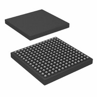
ADSP-21065LCCA-240 Analog Devices Inc, ADSP-21065LCCA-240 Datasheet - Page 14

ADSP-21065LCCA-240
Manufacturer Part Number
ADSP-21065LCCA-240
Description
ADSP-21065 60 Mhz Mini BGA
Manufacturer
Analog Devices Inc
Series
SHARC®r
Type
Fixed/Floating Pointr
Datasheet
1.ADSP-21065LKSZ-240.pdf
(44 pages)
Specifications of ADSP-21065LCCA-240
Rohs Status
RoHS non-compliant
Interface
Host Interface, Serial Port
Clock Rate
60MHz
Non-volatile Memory
External
On-chip Ram
64kB
Voltage - I/o
3.30V
Voltage - Core
3.30V
Operating Temperature
-40°C ~ 100°C
Mounting Type
Surface Mount
Package / Case
196-CSPBGA
Device Core Size
32b
Architecture
Enhanced Harvard
Format
Floating Point
Clock Freq (max)
60MHz
Mips
60
Device Input Clock Speed
60MHz
Ram Size
68KB
Operating Supply Voltage (typ)
3.3V
Operating Supply Voltage (min)
3.13V
Operating Supply Voltage (max)
3.6V
Operating Temp Range
-40C to 100C
Operating Temperature Classification
Industrial
Mounting
Surface Mount
Pin Count
196
Package Type
CSPBGA
Lead Free Status / Rohs Status
Not Compliant
Other names
ADSP-21065LCCA240
Available stocks
Company
Part Number
Manufacturer
Quantity
Price
Company:
Part Number:
ADSP-21065LCCA-240
Manufacturer:
Analog Devices Inc
Quantity:
10 000
ADSP-21065L
Switching Characteristics specify how the processor changes its signals. You have no control over this timing—circuitry external to the
processor must be designed for compatibility with these signal characteristics. Switching characteristics tell you what the processor
will do in a given circumstance. You can also use switching characteristics to ensure that any timing requirement of a device con-
nected to the processor (such as memory) is satisfied.
Timing Requirements apply to signals that are controlled by circuitry external to the processor, such as the data input for a read opera-
tion. Timing requirements guarantee that the processor operates correctly with other devices.
(O/D) = Open Drain
(A/D) = Active Drive
Parameter
Clock Input
Timing Requirements:
t
t
t
t
Parameter
Reset
Timing Requirements:
t
t
NOTES
1
2
Parameter
Interrupts
Timing Requirements:
t
t
t
NOTES
1
2
Applies after the power-up sequence is complete. At power-up, the processor’s internal phase-locked loop requires no more than 3000 CLKIN cycles while RESET is
Only required if multiple ADSP-2106xs must come out of reset synchronous to CLKIN with program counters (PC) equal (i.e., for a SIMD system). Not required
Only required for IRQx recognition in the following cycle.
Applies only if t
CK
CKL
CKH
CKRF
WRST
SRST
low, assuming stable V
for multiple ADSP-2106xs communicating over the shared bus (through the external port), because the bus arbitration logic synchronizes itself automatically after
reset.
SIR
HIR
IPW
SIR
CLKIN Period
CLKIN Width Low
CLKIN Width High
CLKIN Rise/Fall (0.4 V–2.0 V)
RESET Pulsewidth Low
RESET Setup Before CLKIN High
IRQ2-0 Setup Before CLKIN High or Low
IRQ2-0 Hold Before CLKIN High or Low
IRQ2-0 Pulsewidth
and t
DD
HIR
and CLKIN (not including start-up time of external clock oscillator).
requirements are not met.
RESET
CLKIN
2
1
CLKIN
2
Figure 7. Clock Input
1
Figure 8. Reset
Min
30.00
7.0
5.0
1
t
CKH
–14–
66 MHz
t
WRST
t
CK
Max
100
3.0
t
CKL
t
SRST
Min
Min
2 t
23.5 + 24 DT t
Min
11.0 + 12 DT
2.0 + t
33.33
7.0
5.0
CK
60 MHz
CK
/2
Max
100
3.0
Max
Max
0.0 + 12 DT
CK
REV. C
Unit
ns
Unit
ns
ns
Unit
ns
ns
ns
ns
ns
ns


