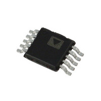
ADP1873ARMZ-0.3-R7 Analog Devices Inc, ADP1873ARMZ-0.3-R7 Datasheet - Page 21

ADP1873ARMZ-0.3-R7
Manufacturer Part Number
ADP1873ARMZ-0.3-R7
Description
300kHz, Light Load Eff Enabled
Manufacturer
Analog Devices Inc
Datasheet
1.ADP1872ARMZ-0.6-R7.pdf
(40 pages)
Specifications of ADP1873ARMZ-0.3-R7
Pwm Type
Current Mode
Number Of Outputs
1
Frequency - Max
300kHz
Duty Cycle
84%
Voltage - Supply
2.75 V ~ 20 V
Buck
Yes
Boost
No
Flyback
No
Inverting
No
Doubler
No
Divider
No
Cuk
No
Isolated
No
Operating Temperature
-40°C ~ 125°C
Package / Case
10-MSOP, Micro10™, 10-uMAX, 10-uSOP
Frequency-max
300kHz
Lead Free Status / RoHS Status
Lead free / RoHS Compliant
Other names
ADP1873ARMZ-0.3-R7TR
Available stocks
Company
Part Number
Manufacturer
Quantity
Price
Company:
Part Number:
ADP1873ARMZ-0.3-R7
Manufacturer:
Analog Devices Inc
Quantity:
1 900
SYNCHRONOUS RECTIFIER
The ADP1872/ADP1873 employ an internal lower side MOSFET
driver to drive the external upper side and lower side MOSFETs.
The synchronous rectifier not only improves overall conduction
efficiency but also ensures proper charging to the bootstrap
capacitor located at the upper side driver input. This is beneficial
during startup to provide sufficient drive signal to the external
upper side MOSFET and attain fast turn-on response, which is
essential for minimizing switching losses. The integrated upper
and lower side MOSFET drivers operate in complementary
fashion with built-in anticross conduction circuitry to prevent
unwanted shoot-through current that may potentially damage the
MOSFETs or reduce efficiency as a result of excessive power loss.
POWER SAVING MODE (PSM) VERSION (ADP1873)
The power saving mode version of the ADP1872 is the ADP1873.
The ADP1873 operates in the discontinuous conduction mode
(DCM) and pulse skips at light load to midload currents. It
outputs pulses as necessary to maintain output regulation. Unlike
the continuous conduction mode (CCM), DCM operation
prevents negative current, thus allowing improved system
efficiency at light loads. Current in the reverse direction through
this pathway, however, results in power dissipation and therefore
a decrease in efficiency.
To minimize the chance of negative inductor current buildup,
an on-board, zero-cross comparator turns off all upper side
and lower side switching activities when the inductor current
approaches the zero current line, causing the system to enter
idle mode, where the upper side and lower side MOSFETs are
turned off. To ensure idle mode entry, a 10 mV offset, connected
in series at the SW node, is implemented (see Figure 74).
I
LOAD
HS
LS
0A
Figure 74. Zero-Cross Comparator with 10 mV of Offset
t
Figure 73. Discontinuous Mode of Operation (DCM)
ON
COMPARATOR
ZERO-CROSS
t
OFF
LS
10mV
AS THE INDUCTOR
CURRENT APPROACHES
ZERO CURRENT, THE STATE
MACHINE TURNS OFF THE
LOWER SIDE MOSFET.
SW
Q2
HS AND LS ARE OFF
OR IN IDLE MODE
I
Q2
Rev. A | Page 21 of 40
As soon as the forward current through the lower side MOSFET
decreases to a level where
the zero-cross comparator (or I
turn off the lower side MOSFET. From this point, the slope of the
inductor current ramping down becomes steeper (see Figure 75)
as the body diode of the lower side MOSFET begins to conduct
current and continues conducting current until the remaining
energy stored in the inductor has been depleted.
The system remains in idle mode until the output voltage drops
below regulation. A PWM pulse is then produced, turning on the
upper side MOSFET to maintain system regulation. The ADP1873
does not have an internal clock; therefore, it switches purely as a
hysteretic controller, as described in this section.
TIMER OPERATION
The ADP1872/ADP1873 employ a constant on-time architecture,
which provides a variety of benefits, including improved load
and line transient response when compared with a constant
(fixed) frequency current-mode control loop of comparable
loop design. The constant on-time timer, or t
the high input voltage (VIN) and the output voltage (V
SW waveform information to produce an adjustable one-shot
PWM pulse that varies the on-time of the upper side MOSFET in
response to dynamic changes in input voltage, output voltage, and
load current conditions to maintain regulation. It then generates
an on-time (t
where K is a constant that is trimmed using an RC timer product
for the 300 kHz, 600 kHz, and 1.0 MHz frequency options.
Figure 75. 10 mV Offset to Ensure Prevention of Negative Inductor Current
10 mV = I
t
I
LOAD
ON
SW
LS
0A
=
K
ON
×
Q2
V
) pulse that is inversely proportional to V
VIN
OUT
× R
ANOTHER
TRIGGERED WHEN V
FALLS BELOW REGULATION
ON(Q2)
ZERO-CROSS COMPARATOR
DETECTS 10mV OFFSET AND
TURNS OFF LS
10mV = R
t
ON
REV
EDGE IS
ON
ADP1872/ADP1873
comparator) emits a signal to
× I
OUT
LOAD
IN IDLE MODE
HS AND LS
ON
timer, senses
t
ON
OUT
) using
IN
.


