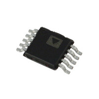
ADP1873ARMZ-0.3-R7 Analog Devices Inc, ADP1873ARMZ-0.3-R7 Datasheet - Page 18

ADP1873ARMZ-0.3-R7
Manufacturer Part Number
ADP1873ARMZ-0.3-R7
Description
300kHz, Light Load Eff Enabled
Manufacturer
Analog Devices Inc
Datasheet
1.ADP1872ARMZ-0.6-R7.pdf
(40 pages)
Specifications of ADP1873ARMZ-0.3-R7
Pwm Type
Current Mode
Number Of Outputs
1
Frequency - Max
300kHz
Duty Cycle
84%
Voltage - Supply
2.75 V ~ 20 V
Buck
Yes
Boost
No
Flyback
No
Inverting
No
Doubler
No
Divider
No
Cuk
No
Isolated
No
Operating Temperature
-40°C ~ 125°C
Package / Case
10-MSOP, Micro10™, 10-uMAX, 10-uSOP
Frequency-max
300kHz
Lead Free Status / RoHS Status
Lead free / RoHS Compliant
Other names
ADP1873ARMZ-0.3-R7TR
Available stocks
Company
Part Number
Manufacturer
Quantity
Price
Company:
Part Number:
ADP1873ARMZ-0.3-R7
Manufacturer:
Analog Devices Inc
Quantity:
1 900
ADP1872/ADP1873
THEORY OF OPERATION
The ADP1872/ADP1873 are versatile current-mode, synchronous
step-down controllers that provide superior transient response,
optimal stability, and current limit protection by using a constant
on-time, pseudo-fixed frequency with a programmable current-
sense gain, current-control scheme. In addition, these devices offer
optimum performance at low duty cycles by using valley current-
mode control architecture. This allows the ADP1872/
ADP1873 to drive all N-channel power stages to regulate output
voltages as low as 0.6 V.
STARTUP
The ADP1872/ADP1873 have an input low voltage pin (VDD) for
biasing and supplying power for the integrated MOSFET drivers. A
bypass capacitor should be located directly across the VDD (Pin 5)
and PGND (Pin 7) pins. Included in the power-up sequence is
the biasing of the current-sense amplifier, the current-sense gain
circuit (see the Programming Resistor (RES) Detect Circuit
section), the soft start circuit, and the error amplifier.
The current-sense blocks provide valley current information
(see the Programming Resistor (RES) Detect Circuit section)
and are a variable of the compensation equation for loop stability
(see the Compensation Network section). The valley current
information is extracted by forcing 0.4 V across the DRVL output
and the PGND pin, which generates a current depending on the
resistor across DRVL and PGND in a process performed by the
RES detect circuit. The current through the resistor is used to set
the current-sense amplifier gain. This process takes approximately
800 μs, after which the drive signal pulses appear at the DRVL
and DRVH pins synchronously and the output voltage begins to
rise in a controlled manner through the soft start sequence.
The rise time of the output voltage is determined by the soft start
and error amplifier blocks (see the Soft Start section). At the
beginning of a soft start, the error amplifier charges the external
compensation capacitor, causing the COMP/EN pin to rise above the
enable threshold of 285 mV, thus enabling the ADP1872/ADP1873.
SOFT START
The ADP1872/ADP1873 have digital soft start circuitry, which
involves a counter that initiates an incremental increase in current,
by 1 μA, via a current source on every cycle through a fixed internal
capacitor. The output tracks the ramping voltage by producing
PWM output pulses to the upper side MOSFET. The purpose is to
limit the in-rush current from the high voltage input supply (VIN)
to the output (V
PRECISION ENABLE CIRCUITRY
The ADP1872/ADP1873 employ precision enable circuitry. The
enable threshold is 285 mV typical with 35 mV of hysteresis.
The devices are enabled when the COMP/EN pin is released,
allowing the error amplifier output to rise above the enable
threshold (see Figure 65). Grounding this pin disables the
ADP1872/ADP1873, reducing the supply current of the devices
to approximately 140 μA. For more information, see Figure 66.
OUT
).
Rev. A | Page 18 of 40
UNDERVOLTAGE LOCKOUT
The undervoltage lockout (UVLO) feature prevents the part
from operating both the upper side and lower side MOSFETs
at extremely low or undefined input voltage (VDD) ranges.
Operation at an undefined bias voltage may result in the incorrect
propagation of signals to the high-side power switches. This, in
turn, results in invalid output behavior that can cause damage
to the output devices, ultimately destroying the device tied at
the output. The UVLO level has been set at 2.65 V (nominal).
THERMAL SHUTDOWN
The thermal shutdown is a self-protection feature to prevent the IC
from damage due to a very high operating junction temperature.
If the junction temperature of the device exceeds 155°C, the
part enters the thermal shutdown state. In this state, the device
shuts off both the upper side and lower side MOSFETs and
disables the entire controller immediately, thus reducing the
power consumption of the IC. The part resumes operation after
the junction temperature of the part cools to less than 140°C.
Figure 65. Release COMP/EN Pin to Enable the ADP1872/ADP1873
500mV
285mV
>2.4V
2.4V
1.0V
COMP/EN
0V
R
C
C
COMP/EN
C
Figure 66. COMP/EN Voltage Range
C
C2
FB
HICCUP MODE INITIALIZED
MAXIMUM CURRENT (UPPER CLAMP)
PRECISION ENABLE THRESHOLD
ZERO CURRENT
LOWER CLAMP
35mV HYSTERESIS
USABLE RANGE ONLY AFTER SOFT START
PERIOD IF CONTUNUOUS CONDUCTION
MODE OF OPERATION IS SELECTED.
ADP1872/ADP1873
ERROR
AMPLIFIER
285mV
V
DD
PRECISION
ENABLE
TO ENABLE
ALL BLOCKS
SS
0.6V


