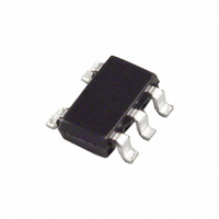
ADP150AUJZ-1.8-R7 Analog Devices Inc, ADP150AUJZ-1.8-R7 Datasheet - Page 11

ADP150AUJZ-1.8-R7
Manufacturer Part Number
ADP150AUJZ-1.8-R7
Description
150mA Ultra-Low Noise LDO 1.8 Vout
Manufacturer
Analog Devices Inc
Datasheet
1.ADP150-BL1-EVZ.pdf
(20 pages)
Specifications of ADP150AUJZ-1.8-R7
Design Resources
Broadband Low EVM Direct Conversion Transmitter (CN0134) Broadband Low EVM Direct Conversion Transmitter Using LO Divide-by-2 Modulator (CN0144) Using low noise linear drop-out regulators to power wideband PLL & VCO IC's (CN0147)
Regulator Topology
Positive Fixed
Voltage - Output
1.8V
Voltage - Input
2.2 ~ 5.5 V
Voltage - Dropout (typical)
0.105V @ 150mA
Number Of Regulators
1
Current - Output
150mA (Max)
Current - Limit (min)
190mA
Operating Temperature
-40°C ~ 125°C
Mounting Type
Surface Mount
Package / Case
TSOT-23-5, TSOT-5, TSOP-5
Lead Free Status / RoHS Status
Lead free / RoHS Compliant
Other names
ADP150AUJZ-1.8-R7TR
Available stocks
Company
Part Number
Manufacturer
Quantity
Price
Part Number:
ADP150AUJZ-1.8-R72
Manufacturer:
ADI/亚德诺
Quantity:
20 000
THEORY OF OPERATION
The ADP150 is an ultralow noise, low quiescent current, low
dropout linear regulator that operates from 2.2 V to 5.5 V and
can provide up to 150 mA of output current. Drawing a low 220 µA
of quiescent current (typical) at full load makes the ADP150 ideal
for battery-operated portable equipment. Shutdown current
consumption is typically 200 nA.
Using new innovative design techniques, the ADP150 provides
superior noise performance for noise sensitive analog and
RF applications without the need for a noise bypass capacitor.
The ADP150 is also optimized for use with small 1 µF ceramic
capacitors.
GND
VIN
EN
SHUTDOWN
Figure 26. Internal Block Diagram
SHORT CIRCUIT,
UVLO, AND
THERMAL
PROTECT
REFERENCE
VOLTAGE
R1
R2
VOUT
Rev. A | Page 11 of 20
Internally, the ADP150 consists of a reference, an error amplifier,
a feedback voltage divider, and a PMOS pass transistor. Output
current is delivered via the PMOS pass device that is controlled
by the error amplifier. The error amplifier compares the reference
voltage with the feedback voltage from the output and amplifies
the difference. If the feedback voltage is lower than the reference
voltage, the gate of the PMOS device is pulled lower, allowing
more current to pass and increasing the output voltage. If the
feedback voltage is higher than the reference voltage, the gate of
the PMOS device is pulled higher, allowing less current to pass
and decreasing the output voltage.
The ADP150 is available in 14 output voltage options, ranging
from 1.8 V to 3.3 V. The ADP150 uses the EN pin to enable and
disable the VOUT pin under normal operating conditions. When
EN is high, VOUT turns on, and when EN is low, VOUT turns
off. For automatic startup, EN can be tied to VIN.
ADP150


