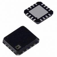
ADN2892ACPZ-RL Analog Devices Inc, ADN2892ACPZ-RL Datasheet - Page 11

ADN2892ACPZ-RL
Manufacturer Part Number
ADN2892ACPZ-RL
Description
IC,Application Specific Amplifier,SINGLE,LLCC,16PIN,PLASTIC
Manufacturer
Analog Devices Inc
Datasheet
1.ADN2892ACPZ-RL.pdf
(16 pages)
Specifications of ADN2892ACPZ-RL
Amplifier Type
Limiting
Number Of Circuits
1
-3db Bandwidth
1.5GHz
Voltage - Input Offset
100µV
Current - Supply
48mA
Voltage - Supply, Single/dual (±)
2.9 V ~ 3.6 V
Operating Temperature
-40°C ~ 95°C
Mounting Type
Surface Mount
Package / Case
16-LFCSP
Lead Free Status / RoHS Status
Lead free / RoHS Compliant
Output Type
-
Current - Output / Channel
-
Slew Rate
-
Gain Bandwidth Product
-
Current - Input Bias
-
Lead Free Status / RoHS Status
Lead free / RoHS Compliant
APPLICATIONS
PCB DESIGN GUIDELINES
Proper RF PCB design techniques must be used to ensure
optimal performance.
Output Buffer Power Supply and Ground Planes
Pin 9 (DRVEE) and Pin 12 (DRVCC) are the power supply and
ground pins that provide current to the differential output
buffer. To reduce possible series inductance, Pin 9, which is the
ground return of the output buffer, should connect to ground
directly. If the ground plane is an internal plane and
connections to the ground plane are vias, multiple vias in
parallel to ground can reduce series inductance.
Similarly, to reduce the possible series inductance, Pin 12,
which supplies power to the high speed differential
OUTP/OUTN output buffer, should connect to the power plane
directly. If the power plane is an internal plane and connections
to the power plane are vias, multiple vias in parallel can reduce
the series inductance, especially on Pin 12. See Figure 18 for the
recommended connections.
ADN2882
VCC
VCC
0.1µF
C5
C1
C2
C6
AVCC
AVEE
NIN
C12
PIN
Figure 18. Typical ADN2892 Applications Circuit
1
2
3
4
16
5
R2
ADN2892
CONNECT
VCC
EXPOSED
15
PAD TO
6
Rev. 0 | Page 11 of 16
GND
14
7
C9
VCC
13
8
R3
4.7kΩ TO 10kΩ
ON HOST BOARD
12
10
11
9
The exposed pad should connect to the GND plane using filled
vias so that solder does not leak through the vias during reflow.
Using filled vias in parallel under the package greatly reduces
the thermal resistance and enhances the reliability of the
connectivity of the exposed pad to the GND plane during
reflow.
To reduce power supply noise, a 10 µF electrolytic decoupling
capacitor between power and ground should be close to where
the 3.3 V supply enters the PCB. The other 0.1 µF and 1 nF
ceramic chip decoupling capacitors should be close to the VCC
and VEE pins to provide optimal supply decoupling and a
shorter current return loop.
R1
DRVCC
OUTP
OUTN
DRVEE
C1–C4, C11: 0.01µF X5R/X7R DIELECTRIC, 0201 CASE
C5, C7, C9, C10, C12: 0.1µF X5R/X7R DIELECTRIC, 0402 CASE
C6, C8: 1nF X5R/X7R DIELECTRIC, 0201 CASE
C10
C3
C4
RSSI MEASUREMENT
TO ADC
TO ADuC7020
C7
TO HOST
BOARD
VCC
C8
ADN2892


