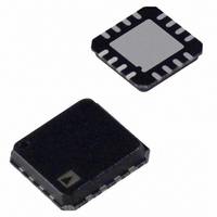
ADN2892ACPZ-RL Analog Devices Inc, ADN2892ACPZ-RL Datasheet

ADN2892ACPZ-RL
Specifications of ADN2892ACPZ-RL
Related parts for ADN2892ACPZ-RL
ADN2892ACPZ-RL Summary of contents
Page 1
FEATURES Input sensitivity: 3 rise/fall times CML outputs: 750 mV p-p differential Bandwidth selectable for multirate 1×/2×/4× FC modules Optional LOS output inversion Programmable LOS detector: 3 signal strength indicator (RSSI) ...
Page 2
ADN2892 TABLE OF CONTENTS Specifications..................................................................................... 3 Absolute Maximum Ratings............................................................ 5 Thermal Resistance ...................................................................... 5 ESD Caution.................................................................................. 5 Pin Configuration and Function Descriptions............................. 6 Typical Performance Characteristics ............................................. 7 Theory of Operation ...................................................................... 10 Limiting Amplifier ..................................................................... 10 Loss-of-Signal (LOS) Detector ...
Page 3
SPECIFICATIONS Test Conditions: VCC = 2 3.6 V, VEE = Table 1. Parameter QUANTIZER DC CHARACTERISTICS Input Voltage Range Input Common Mode Peak-to-Peak Differential Input Range Input Sensitivity Input Offset Voltage Input RMS Noise Input ...
Page 4
ADN2892 Parameter LOGIC INPUTS (SQUELCH, LOS_INV, AND BW_SEL Input High Voltage Input Low Voltage IL Input Current (SQUELCH, LOS_INV) Input Current (BW_SEL) LOGIC OUTPUTS (LOS Output High Voltage Output Low ...
Page 5
ABSOLUTE MAXIMUM RATINGS Table 2. Parameter Power Supply Voltage Minimum Voltage (All Inputs and Outputs) Maximum Voltage (All Inputs and Outputs) Storage Temperature Operating Temperature Range Production Soldering Temperature Junction Temperature ESD CAUTION ESD (electrostatic discharge) sensitive device. Electrostatic charges ...
Page 6
ADN2892 PIN CONFIGURATION AND FUNCTION DESCRIPTIONS Note that there is an exposed pad on the bottom of the package that must be connected to the GND plane with filled vias. Table 4. Pin Function Descriptions Pin No. Mnemonic I/O Type ...
Page 7
TYPICAL PERFORMANCE CHARACTERISTICS 50ps/DIV Figure 3. Eye of ADN2892 @ 25°C, 4.25 Gbps, and 10 mV Input 50ps/DIV Figure 4. Eye of ADN2892 @ 95°C, 4.25 Gbps, and 10 mV Input 200ps/DIV Figure 5. Eye of ADN2892 at 25°C, 1.063 ...
Page 8
ADN2892 4.0 3.5 3.0 2.5 2.0 1.5 1.0 0.5 0 1.0 1.5 2.0 2.5 3.0 RATE (Gbps) Figure 9. Random Jitter vs. Data Rate 1.0 1.5 2.0 2.5 3.0 RATE ...
Page 9
TEMPERATURE (°C) Figure 15. RSSI Offset—Difference Between Measured RSSI Output and PD_CATHODE (Input) Current of 5 µA 5.0 4.5 4.0 3.5 3.0 2.5 +100 ° ...
Page 10
ADN2892 THEORY OF OPERATION LIMITING AMPLIFIER Input Buffer The ADN2892 limiting amplifier provides differential inputs (PIN/NIN), each with a single-ended, on-chip 50 Ω termination. The amplifier can accept either dc-coupled or ac-coupled signals; however, an ac-coupled signal is recommended. Using ...
Page 11
APPLICATIONS PCB DESIGN GUIDELINES Proper RF PCB design techniques must be used to ensure optimal performance. Output Buffer Power Supply and Ground Planes Pin 9 (DRVEE) and Pin 12 (DRVCC) are the power supply and ground pins that provide current ...
Page 12
ADN2892 PCB Layout Figure 19 shows the recommended PCB layout. The 50 Ω transmission lines are the traces that bring the high frequency input and output signals (PIN, NIN, OUTP, and OUTN) from a terminated source to a terminated load ...
Page 13
... MAX 0.90 0.85 0.80 SEATING PLANE ORDERING GUIDE Model Temperature Range ADN2892ACPZ-500RL7 1 –40°C to +95°C 1 ADN2892ACPZ-RL7 –40°C to +95°C ADN2892ACPZ-RL 1 –40°C to +95°C EVAL-ADN2892EB Pb-free part. 3.00 0.60 MAX BSC SQ 0.45 2.75 TOP BSC SQ VIEW 0.50 BSC 1 ...
Page 14
ADN2892 NOTES Rev Page ...
Page 15
NOTES Rev Page ADN2892 ...
Page 16
ADN2892 NOTES ©2005 Analog Devices, Inc. All rights reserved. Trademarks and registered trademarks are the property of their respective owners. D04986–0–4/05(0) Rev Page ...


