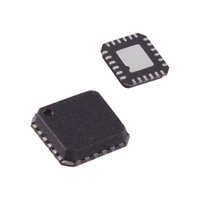
ADN2871ACPZ-RL7 Analog Devices Inc, ADN2871ACPZ-RL7 Datasheet

ADN2871ACPZ-RL7
Specifications of ADN2871ACPZ-RL7
Related parts for ADN2871ACPZ-RL7
ADN2871ACPZ-RL7 Summary of contents
Page 1
FEATURES SFP/SFF and SFF-8472 MSA-compliant SFP reference design available 50 Mbps to 4.25 Gbps operation Automatic average power control Typical rise/fall time 60 ps Supports VCSEL, DFB, and FP lasers Bias current range 100 mA Modulation current ...
Page 2
ADN2871 TABLE OF CONTENTS Features .............................................................................................. 1 Applications....................................................................................... 1 General Description ......................................................................... 1 Revision History ............................................................................... 2 Specifications..................................................................................... 3 SFP Timing Specifications............................................................... 5 Absolute Maximum Ratings............................................................ 6 ESD Caution.................................................................................. 6 Pin Configuration and Function Descriptions............................. 7 Optical Waveforms ........................................................................... 8 ...
Page 3
SPECIFICATIONS 3.6 V. All specifications T CC Table 1. Parameter LASER BIAS CURRENT (IBIAS) Output Current (IBIAS) Compliance Voltage IBIAS when ALS is High MODULATION CURRENT (IMODP, IMODN) Output Current (IMOD) Compliance Voltage IMOD when ...
Page 4
ADN2871 Parameter 9 ALARM OUTPUT (FAIL) V OFF V ON IBMON/IMMON DIVISION RATIO 3 IBIAS/IBMON 3 IBIAS/IBMON 3 IBIAS/IBMON 3, 10 IBIAS/IBMON Stability IMOD/IMMON IBMON Compliance Voltage SUPPLY (with respect to GND Temperature ...
Page 5
SFP TIMING SPECIFICATIONS Table 2. Parameter ALS Assert Time 1 ALS Negate Time 1 Time to Initialize, Including Reset of FAIL FAIL Assert Time ALS to Reset Time 1 Guaranteed by design and characterization. Not production tested. Symbol Min Typ ...
Page 6
ADN2871 ABSOLUTE MAXIMUM RATINGS Table 3. Parameter V to GND CC IMODN, IMODP All Other Pins Junction Temperature Operating Temperature Range Industrial Storage Temperature Range Junction Temperature (T max) J LFCSP 1 Power Dissipation 2 θ Thermal Impedance JA θ ...
Page 7
PIN CONFIGURATION AND FUNCTION DESCRIPTIONS Note: The LFCSP has an exposed paddle that must be connected to ground. Table 4. Pin Function Descriptions Pin No. Mnemonic Description 1 CCBIAS In ac-coupled mode, CCBIAS can connect to either IBIAS or V ...
Page 8
ADN2871 OPTICAL WAVEFORMS V = 3.3 V and T = 25°C, unless otherwise noted. Note: No change to PAVCAP and ERCAP values MULTIRATE PERFORMANCE USING LOW COST FABRY PEROT TOSA NEC NX7315UA (ACQ LIMIT TEST) WAVEFORMS 1000 Figure ...
Page 9
TYPICAL PERFORMANCE CHARACTERISTICS SINGLE-ENDED OUTPUT These performance characteristics were measured using the high speed, electrical single-ended, output circuit shown in Figure MODULATION CURRENT (mA) Figure 12. Rise Time vs. Modulation Current, ...
Page 10
ADN2871 DIFFERENTIAL OUTPUT These performance characteristics were measured using the high speed, electrical differential output circuit shown in Figure MODULATION CURRENT (mA) Figure 16. Rise Time vs. Modulation Current ...
Page 11
PERFORMANCE CHARACTERISTICS 250 220 I = 80mA BIAS 190 I BIAS 160 130 100 MODULATION CURRENT (mA) Figure 20. Total Supply Current vs. Modulation Current Total Supply Current = 120 ...
Page 12
ADN2871 FAIL ASSERTED FAULT FORCED ON PAVSET Figure 26. FAIL Assert Time,1 μs/DIV Figure 27. Time to Initialize, Including Reset, 40 ms/DIV Rev Page TRANSMISSION ON POWER SUPPLY TURN ON ...
Page 13
THEORY OF OPERATION Laser diodes have a current-in to light-out transfer function, as shown in Figure 28. Two key characteristics of this transfer function are the threshold current, Ith, and the slope in the linear region beyond the threshold current, ...
Page 14
ADN2871 Tx_DISABLE Tx_FAULT ADI MICROCONTROLLER DAC ADC DAC Figure 29. ADN2871 Using Microconverter Voltage Setpoint Calibration and Monitoring PAVREF MPD PAVSET V GND CC ERREF ERSET GND Figure 30. ADN2871 Using Resistor Setpoint Calibration of Average ...
Page 15
RESISTOR SETPOINT CALIBRATION In resistor setpoint calibration, Pin PAVREF, Pin ERREF, and Pin RPAV must all be tied The average power and CC extinction ratio can be set using the PAVSET and ERSET pins, respectively. A resistor ...
Page 16
ADN2871 Resistor Setpoint In resistor setpoint calibration, the current through the resistor from PAVSET to ground is the I current. The recommended MPD method for measuring the I current is to place a small MPD resistor in series with the ...
Page 17
DATA INPUTS Data inputs should be ac-coupled (10 nF capacitors are recommended) and are terminated via a 100 Ω internal resistor between the DATAP and DATAN pins. A high impedance circuit sets the common-mode voltage and is designed to allow ...
Page 18
ADN2871 ALARMS The ADN2871 has a latched, active high monitoring alarm (FAIL). The FAIL alarm output is an open drain in conformance to SFP MSA specification requirements. The ADN2871 has a three-fold alarm system that covers • Use of a ...
Page 19
... MAX 0.85 0.80 SEATING PLANE ORDERING GUIDE Model Temperature Range 1 ADN2871ACPZ −40°C to +85°C 1 ADN2871ACPZ-RL −40°C to +85°C 1 ADN2871ACPZ-RL7 −40°C to +85° Pb-free part. 0.60 MAX 4.00 BSC SQ 0.60 MAX 19 0.50 18 BSC TOP 3.75 EXPOSED VIEW ...
Page 20
ADN2871 NOTES ©2007 Analog Devices, Inc. All rights reserved. Trademarks and registered trademarks are the property of their respective owners. D05228-0-2/07(A) Rev Page ...


