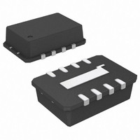
ADL5315ACPZ-R7 Analog Devices Inc, ADL5315ACPZ-R7 Datasheet

ADL5315ACPZ-R7
Specifications of ADL5315ACPZ-R7
Related parts for ADL5315ACPZ-R7
ADL5315ACPZ-R7 Summary of contents
Page 1
FEATURES Accurately mirrors input current (1:1 ratio) over 6 decades Linearity 1% from Stable mirror input voltage Voltage held 1 V below supply using internal reference or can be set externally Adjustable input current limit ...
Page 2
ADL5315 TABLE OF CONTENTS Features .............................................................................................. 1 Applications....................................................................................... 1 Functional Block Diagram .............................................................. 1 General Description ......................................................................... 1 Revision History ............................................................................... 2 Specifications..................................................................................... 3 Absolute Maximum Ratings............................................................ 4 ESD Caution.................................................................................. 4 Pin Configuration and Function Descriptions............................. 5 Typical Performance Characteristics ...
Page 3
SPECIFICATIONS μ 25°C, unless otherwise noted. POS SET INPT A Table 1. Parameter CURRENT MIRROR OUTPUT Current Gain from INPT to IOUT Current Gain from INPT to ...
Page 4
ADL5315 ABSOLUTE MAXIMUM RATINGS Table 2. Parameter Supply Voltage Input Current at INPT Internal Power Dissipation θ (Soldered Exposed Paddle) JA Maximum Junction Temperature Operating Temperature Range Storage Temperature Range Lead Temperature (Soldering 60 sec) ESD CAUTION ESD (electrostatic discharge) ...
Page 5
PIN CONFIGURATION AND FUNCTION DESCRIPTIONS Table 3. Pin Function Descriptions Pin No. Mnemonic Description 1 INPT Input Current. Pin sources current only. 2 VSET Sets Voltage at INPT (Gain = 1). Range − ...
Page 6
ADL5315 TYPICAL PERFORMANCE CHARACTERISTICS 25°C, unless otherwise noted. POS SET SREF OUT A 2.0 +25°C, +70°C, +85°C, –40°C 0°C 0°C, –40°C 1.5 +25°C +70°C +85°C 1.0 ...
Page 7
SIGMA 10 5 AVERAGE 0 –5 –10 –3 SIGMA –15 –20 –40 –30 –20 – TEMPERATURE (°C) Figure 9. Temperature Drift of V with INPT SET ...
Page 8
ADL5315 1.010 1.005 +85 +25 1.000 –40 0.995 0.990 (V) POS Figure 15. V − V vs. V for Multiple Temperatures POS INPT POS 0.99 0.993 0.996 0.999 1.002 ...
Page 9
THEORY OF OPERATION The ADL5315 addresses the need for precision high-side monitoring of photodiode current in fiber optic systems and is useful in many nonoptical applications as well optimized for use with ADI’s family of translinear logarithmic amplifiers, ...
Page 10
ADL5315 The VSET control is intended primarily to provide a dc bias voltage for the mirror input, but it is also well behaved in the presence of the V transients. The rise time of V SET independent of input current ...
Page 11
APPLICATIONS The ADL5315 is primarily designed for wide dynamic range applications, simplifying power monitoring designs where access is only permitted to the cathode of a PIN photodiode or receiver module. Figure 22 shows a typical application where the ADL5315 is ...
Page 12
ADL5315 TRANSLINEAR LOG AMP INTERFACING The mirror current output, IOUT, of the ADL5315 is designed to interface directly to an Analog Devices translinear logarithmic amplifier, such as the AD8304, AD8305, or ADL5306. Figure 24 shows the basic connections necessary for ...
Page 13
EXTENDED OPERATING RANGE The ADL5315 is specified over an input current range mA, but the device remains fully functional over the full eight decade range specified for ADI’s flagship translinear logarithmic amplifier, the AD8304 (100 ...
Page 14
ADL5315 2.2 2.0 1.8 1.6 1.4 1.2 1.0 0.8 0.6 0.4 0.2 0 100p 1n 10n 100n 1μ 10μ I (A) INPT Figure 28. V Voltage vs. I SET RLIM Is Configured for Automatic Photodiode Biasing 2.2 2.0 1.8 1.6 ...
Page 15
Figure 31. Configuration for Noise Spectral Density and Wideband Current Noise Figure 32 shows the configuration used to measure the pulse response create the test ...
Page 16
ADL5315 EVALUATION BOARD L1 0Ω OPEN 390pF V SET Table 4. Evaluation Board (Rev. A) Configuration Options Component Function VPOS, GND Supply and ground connections. INPUT, L1, C4 Input Interface: The evaluation board is configured to accept ...
Page 17
... OUTLINE DIMENSIONS PIN 1 INDICATOR 1.00 0.85 0.80 SEATING ORDERING GUIDE Model Temperature Range 1 ADL5315ACPZ-R7 –40°C to +85°C ADL5315ACPZ- –40°C to +85°C ADL5315-EVAL Pb-free part Waffle pack 3.25 3.00 2.75 0.60 0.45 2.25 1.95 0.30 2.00 TOP VIEW 1.75 1.75 1 ...
Page 18
ADL5315 NOTES Rev Page ...
Page 19
NOTES Rev Page ADL5315 ...
Page 20
ADL5315 NOTES © 2005 Analog Devices, Inc. All rights reserved. Trademarks and registered trademarks are the property of their respective owners. D05694–0–10/05(0) Rev Page ...


