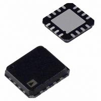
ADL5306ACPZ-REEL7 Analog Devices Inc, ADL5306ACPZ-REEL7 Datasheet - Page 9

ADL5306ACPZ-REEL7
Manufacturer Part Number
ADL5306ACPZ-REEL7
Description
60db Log
Manufacturer
Analog Devices Inc
Type
Logarithmic Converterr
Datasheet
1.ADL5306ACP-R2.pdf
(16 pages)
Specifications of ADL5306ACPZ-REEL7
Design Resources
Interfacing ADL5315 to Translinear Logarithmic Amplifier (CN0056) Interfacing ADL5317 High Side Current Mirror to a Translinear Logarithmic Amplifier in an Avalanche Photodiode Power Detector
Applications
Fiber Optics
Mounting Type
Surface Mount
Package / Case
16-LFCSP
Lead Free Status / RoHS Status
Lead free / RoHS Compliant
Other names
ADL5306ACPZ-REEL7
ADL5306ACPZ-REEL7TR
ADL5306ACPZ-REEL7TR
GENERAL STRUCTURE
The ADL5306 addresses a wide variety of interfacing conditions
to meet the needs of fiber optic supervisory systems, and is
useful in many nonoptical applications. This section explains
the structure of this unique style of translinear log amp. The
simplified schematic in Figure 21 shows the key elements.
The photodiode current I
at this node is essentially equal to the voltage on the two
adjacent guard pins, VSUM and IREF, due to the low offset
voltage of the JFET op amp. Transistor Q1 converts I
corresponding logarithmic voltage, as shown in Equation 1. A
finite positive value of V
for the usual case of a single-supply voltage. This is internally
set to 0.5 V, one fifth of the 2.5 V reference voltage appearing on
Pin VREF. The resistance at the VSUM pin is nominally 16 kΩ;
this voltage is not intended as a general bias source.
The ADL5306 also supports the use of an optional negative
supply voltage, V
negative, VSUM may be connected to ground; thus, INPT and
IREF assume this potential. This allows operation as a voltage-
input logarithmic converter by the inclusion of a series resistor
at either or both inputs. Note that the resistor setting, I
need to be adjusted to maintain the intercept value. It should
also be noted that the collector-emitter voltages of Q1 and Q2
are now the full V
errors at large input currents.
The input-dependent V
V
generated externally to a recommended value of 10 µA.
However, other values over a several-decade range can be used
with a slight degradation in law conformance (see Figure 8).
BE2
PHOTODIODE
I
INPT
PD
CURRENT
of a second transistor, Q2, operating at I
INPUT
Q1
0.5V
VNEG (NORMALLY GROUNDED)
VSUM
GENERATOR
80kΩ
2.5V
0.5V
BIAS
N
N
, at Pin VNEG. When V
20kΩ
Figure 21. Simplified Schematic
, and effects due to self-heating will cause
V
VREF
BE1
COMM
BE1
SUM
PD
of Q1 is compared with the reference
IREF
Q2
is received at Pin INPT. The voltage
is needed to bias the collector of Q1
0.5V
I
REF
V
V
V
BE2
BE1
BE2
N
2.5V
is –0.5 V or more
REF
(SUBTRACT AND
COMPENSATION
TEMPERATURE
6.69kΩ
DIVIDE BY T°K)
14.2kΩ
. This is
PD
44µA/dec
451Ω
REF
to a
03727-0-021
COMM
VLOG
, will
Rev. 0 | Page 9 of 16
THEORY
The base-emitter voltage of a BJT (bipolar junction transistor)
can be expressed by the following equation, which immediately
shows its basic logarithmic nature:
where:
I
I
kT/q is the thermal voltage, proportional to absolute
temperature (PTAT), and is 25.85 mV at 300 K.
I
temperature dependence, varying by a factor of roughly a
billion between –35°C and +85°C. Thus, to make use of the BJT
as an accurate logarithmic element, both of these temperature-
dependencies must be eliminated.
The difference between the base-emitter voltages of a matched
pair of BJTs, one operating at the photodiode current I
the other operating at a reference current I
The uncertain, temperature-dependent saturation current, I
that appears in Equation 1 has therefore been eliminated. To
eliminate the temperature variation of kT/q, this difference
voltage is processed by what is essentially an analog divider.
Effectively, it puts a variable under Equation 2. The output of
this process, which also involves a conversion from voltage
mode to current mode, is an intermediate, temperature-
corrected current:
where I
determines the slope of the function (change in current per
decade). For the ADL5306, I
temperature-independent slope of 44 µA/decade for all values
of I
voltage-mode output, V
C
S
S
is a scaling current, typically only 10
is never precisely defined and exhibits an even stronger
is the collector current
V
PD
BE1
V
= 59.5 mV log
I
= ln(10) kT/q log
LOG
and I
BE
– V
Y
= kT/q ln(I
= I
is an accurate, temperature-stable scaling current that
BE2
REF
Y
log
= kT/q ln(I
. This current is subsequently converted back to a
10
(I
10
PD
C
(I
/ I
/ I
10
PD
S
(I
LOG
)
REF
/ I
PD
PD
REF
)
, scaled 200 mV/decade.
/ I
/ I
Y
) (T = 300 K)
S
REF
is 44 µA, resulting in a
) – kT/q ln(I
)
–17
A
REF
REF
, can be written as
/ I
S
)
ADL5306
PD
and
(1)
(2)
(3)
S
,


