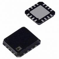
ADL5306ACPZ-REEL7 Analog Devices Inc, ADL5306ACPZ-REEL7 Datasheet - Page 10

ADL5306ACPZ-REEL7
Manufacturer Part Number
ADL5306ACPZ-REEL7
Description
60db Log
Manufacturer
Analog Devices Inc
Type
Logarithmic Converterr
Datasheet
1.ADL5306ACP-R2.pdf
(16 pages)
Specifications of ADL5306ACPZ-REEL7
Design Resources
Interfacing ADL5315 to Translinear Logarithmic Amplifier (CN0056) Interfacing ADL5317 High Side Current Mirror to a Translinear Logarithmic Amplifier in an Avalanche Photodiode Power Detector
Applications
Fiber Optics
Mounting Type
Surface Mount
Package / Case
16-LFCSP
Lead Free Status / RoHS Status
Lead free / RoHS Compliant
Other names
ADL5306ACPZ-REEL7
ADL5306ACPZ-REEL7TR
ADL5306ACPZ-REEL7TR
ADL5306
It is apparent that this output should be zero for I
would need to swing negative for smaller values of input
current. To avoid this, I
smallest value of I
is added to V
intercept to the left by four decades, from 10 µA to 1 nA:
where I
Since values of I
supply of sufficient value is required to accommodate this
situation (discussed later).
The voltage V
resistance of 4.55 kΩ, formed by the parallel combination of a
6.69 kΩ resistor to ground and the 14.2 kΩ resistor to the
internal 2.5 V reference. At the VLOG pin, the output current
I
where V
resistive loading on VLOG will lower this slope and will result
in an overall scaling uncertainty due to the variability of the on-
chip resistors. Consequently, this practice is not recommended.
V
V
pins INPT and IREF may be positioned at ground level simply
by grounding VSUM.
LOG
LOG
N
) are used. When V
generates a voltage of
I
V
= 44 µA × 4.55 kΩ × log
= V
may also swing below ground when dual supplies (V
LOG
LOG
INTC
Y
Y
= I
= I
= 200 mV/decade or 10 mV/dB. Note that any
log
is the operational / value of the intercept current.
Y
LOG
10
LOG
log
LOG
(I
PD
× 4.55 kΩ
10
to shift it upward by 0.8 V. This moves the
PD
is generated by applying I
(I
PD
< I
/ I
PD
. In the ADL5306, an internal offset voltage
INTC
REF
/ I
N
REF
= -0.5 V or more negative, the input
)
INTC
result in a negative V
would need to be as small as the
)
10
(I
PD
/ I
REF
)
LOG
to an internal
LOG
PD
, a negative
= I
REF
, and
P
and
(4)
(5)
Rev. 0 | Page 10 of 16
MANAGING INTERCEPT AND SLOPE
As previously noted, the internally generated 2.5 V bias
combines with the on-chip resistors to introduce an accurate
offset voltage of 0.8 V at the VLOG pin, equivalent to four
decades. This results in a logarithmic transfer function that can
be written as
where I
Thus, the effective intercept current, I
thousandth of I
recommended value of I
The slope can be reduced by attaching a resistor to the VLOG
pin. This is strongly discouraged because the on-chip resistors
will not ratio correctly to the added resistance. Also, it is rare
that one would wish to lower the basic slope of 10 mV/dB; if
this is necessary, it should be done at the low impedance output
of the buffer, which is provided to avoid such miscalibration
and allow higher slopes to be used.
The ADL5306 buffer is essentially an uncommitted op amp
with rail-to-rail output swing, good load driving capabilities,
and a unity-gain bandwidth of >20 MHz. In addition to
allowing the introduction of gain using standard feedback
networks, thereby increasing the slope voltage, V
can be used to implement multipole low-pass filters, threshold
detectors, and a variety of other functions. For more details, see
the AD8304 Data Sheet.
RESPONSE TIME AND NOISE CONSIDERATIONS
The response time and output noise of the ADL5306 are
fundamentally a function of the signal current I
currents, the bandwidth is proportional to I
frequency voltage-noise spectral density is a function of I
increases for small values of I
bandwidth performance of translinear log amps, see the
AD8304 Data Sheet.
V
LOG
INTC
= V
= I
Y
REF
log
REF
/10
, corresponding to 10 nA when using the
10
(10
4
4
REF
× I
PD
= 100 µA.
REF
/ I
. For details of noise and
REF
)= V
INTC
Y
log
, is only one ten-
PD
10
. The output’s low
(I
PD
PD
Y
, the buffer
/ I
. For small
INTC
)
PD
, and
(6)


