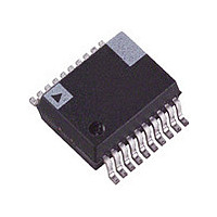
ADG467BRSZ-REEL Analog Devices Inc, ADG467BRSZ-REEL Datasheet - Page 9

ADG467BRSZ-REEL
Manufacturer Part Number
ADG467BRSZ-REEL
Description
Octal Channel Protector I.C.
Manufacturer
Analog Devices Inc
Series
ADG467r
Specifications of ADG467BRSZ-REEL
Voltage - Clamping
±40V
Technology
Mixed Technology
Number Of Circuits
8
Applications
General Purpose
Package / Case
20-SSOP
Operating Temperature (min)
-40C
Operating Temperature (max)
85C
Operating Temperature Classification
Industrial
Mounting
Surface Mount
Pin Count
20
Lead Free Status / RoHS Status
Lead free / RoHS Compliant
Power (watts)
-
Voltage - Working
-
Lead Free Status / Rohs Status
Compliant
Available stocks
Company
Part Number
Manufacturer
Quantity
Price
Part Number:
ADG467BRSZ-REEL
Manufacturer:
ADI/亚德诺
Quantity:
20 000
CIRCUIT INFORMATION
Figure 21 shows a simplified schematic of a channel protector
circuit. The circuit is made up of four MOS transistors—two
NMOS and two PMOS. One of the PMOS devices does not lie
directly in the signal path but is used to connect the source of
the second PMOS device to its backgate. This has the effect of
lowering the threshold voltage and thus increasing the input
signal range of the channel for normal operation. The source
and backgate of the NMOS devices are connected for the same
reason. During normal operation, the channel protectors have
an on resistance of 62 Ω typical. The channel protectors are very
low power devices, and even under fault conditions, the supply
current is limited to sub microampere levels. All transistors are
dielectrically isolated from each other using a trench isolation
method. This makes it impossible to latch up the channel protec-
tors. For further details, see the Trench Isolation section.
OVERVOLTAGE PROTECTION
When a fault condition occurs on the input of a channel protec-
tor, the voltage on the input has exceeded some threshold voltage
set by the supply rail voltages. The threshold voltages are related
to the supply rails as follows. For a positive overvoltage, the
threshold voltage is given by V
voltage of the NMOS transistor (1.5 V typical). In the case of a
negative overvoltage, the threshold voltage is given by V
where V
typical). If the input voltage exceeds these threshold voltages,
TP
is the threshold voltage of the PMOS device (−1.5 V
NMOS
Figure 21. The Channel Protector Circuit
V
DD
OVERVOLTAGE
(SATURATED)
OPERATION
V
DD
SS
V
SS
− V
PMOS
PMOS
(20V)
TN
V
T
, where V
V
= 1.5V
N
Dx
+
SPACE CHARGE
Figure 23. Positive Overvoltages Operation of the Channel Protector
EFFECTIVE
NMOS
REGION
V
DD
TN
is the threshold
P
V
–
N-CHANNEL
G
(V
DD
SS
(V
= 15V)
− V
O
– V
Rev. B | Page 9 of 16
TP
TN
V
N
Sx
,
+
= 13.5V)
(13.5V)
P
the output of the channel protector (no load) is clamped at these
threshold voltages. However, the channel protector output
clamps at a voltage value that is inside these thresholds if the
output is loaded. For example, with an output load of 1 kΩ, V
15 V, and a positive overvoltage on the input, the output clamps
at V
due to an I × R voltage drop across the channels of the MOS
devices (see Figure 23). As can be seen from Figure 23, the current
during fault condition is determined by the load on the output
(that is, V
current is limited to the nano-ampere level.
Figure 22, Figure 24, and Figure 25 show the operating condi-
tions of the signal path transistors during various fault conditions.
Figure 22 shows how the channel protectors operate when a
positive overvoltage is applied to the channel protector.
The first NMOS transistor goes into a saturated mode of
operation as the voltage on its drain exceeds the gate voltage
(V
Figure 23. The potential at the source of the NMOS device is
equal to V
rated mode of operation.
+
OVERVOLTAGE
1
V
TN
DD
DD
= NMOS THRESHOLD VOLTAGE (+1.5V).
) − the threshold voltage (V
POSITIVE
− V
(+20V)
PMOS
Figure 22. Positive Overvoltage on the Channel Protector
NONSATURATED
CLAMP
DD
TN
OPERATION
SATURATED
− V
− ΔV = 15 V − 1.5 V − 0.6 V = 12.9 V, where ΔV is
/R
V
TN
L
). However, if the supplies are off, the fault
NMOS
. The other MOS devices are in a nonsatu-
V
DD
NMOS
(+15V)
I
OUT
SATURATED
R
L
TN
NON-
V
SS
). This situation is shown in
PMOS
V
CLAMP
(–15V)
V
DD
(+13.5V)
SATURATED
– V
TN
1
NON-
V
DD
NMOS
(+15V)
ADG467
DD
=


