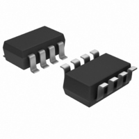
ADG1219BRJZ-REEL7 Analog Devices Inc, ADG1219BRJZ-REEL7 Datasheet - Page 14

ADG1219BRJZ-REEL7
Manufacturer Part Number
ADG1219BRJZ-REEL7
Description
IC,ANALOG SWITCH,SINGLE,SPDT,CMOS,TSSOP,8PIN,PLASTIC
Manufacturer
Analog Devices Inc
Series
iCMOS®r
Type
Analog Switchr
Datasheet
1.ADG1219BRJZ-REEL7.pdf
(16 pages)
Specifications of ADG1219BRJZ-REEL7
Function
Switch
Circuit
1 x SPDT
On-state Resistance
270 Ohm
Voltage Supply Source
Single Supply
Voltage - Supply, Single/dual (±)
12 V ~ 15 V
Current - Supply
1µA
Operating Temperature
-40°C ~ 85°C
Mounting Type
Surface Mount
Package / Case
SOT-23-8
Multiplexer Configuration
Single SPDT
Number Of Inputs
1
Number Of Outputs
2
Number Of Channels
1
Analog Switch On Resistance
475@10.8VOhm
Package Type
SOT-23
Power Supply Requirement
Single/Dual
Single Supply Voltage (typ)
12V
Dual Supply Voltage (typ)
±15V
Mounting
Surface Mount
Pin Count
8
Operating Temp Range
-40C to 125C
Operating Temperature Classification
Automotive
Package
8SOT-23
Maximum On Resistance
475@10.8V Ohm
Maximum Propagation Delay Bus To Bus
170@±15V|250@12V ns
Maximum High Level Output Current
30 mA
Maximum Turn-off Time
185@12V ns
Maximum Turn-on Time
150@12V ns
Switch Architecture
SPDT
Power Supply Type
Single|Dual
Lead Free Status / RoHS Status
Lead free / RoHS Compliant
Lead Free Status / RoHS Status
Lead free / RoHS Compliant
Other names
ADG1219BRJZ-REEL7TR
Available stocks
Company
Part Number
Manufacturer
Quantity
Price
Company:
Part Number:
ADG1219BRJZ-REEL7
Manufacturer:
Allegro
Quantity:
48 573
ADG1219
TERMINOLOGY
I
The positive supply current.
I
The negative supply current.
V
The analog voltage on Terminal D and Terminal S.
R
The ohmic resistance between Terminal D and Terminal S.
R
Flatness is defined as the difference between the maximum and
minimum value of on resistance as measured over the specified
analog signal range.
I
The source leakage current with the switch off.
I
The drain leakage current with the switch off.
I
The channel leakage current with the switch on.
V
The maximum input voltage for Logic 0.
V
The minimum input voltage for Logic 1.
I
The input current of the digital input.
C
The off switch source capacitance, measured with reference
to ground.
C
The off switch drain capacitance, measured with reference
to ground.
C
The on switch capacitance, measured with reference to ground.
C
The digital input capacitance.
DD
SS
S
D
D
INL
ON
FLAT(ON)
S
D
D
IN
D
INL
INH
, I
(Off)
(Off)
, C
(Off)
(V
(Off)
(I
S
(On)
S
INH
S
)
(On)
)
Rev. A | Page 14 of 16
t
Delay time between the 50% and 90% points of the digital input
and switch on condition.
t
Delay time between the 50% and 90% points of the digital input
and switch off condition.
t
Delay time between the 50% and 90% points of the digital
inputs and the switch on condition when switching from one
address state to another.
T
Off time measured between the 80% point of both switches
when switching from one address state to another.
Charge Injection
A measure of the glitch impulse transferred from the digital
input to the analog output during switching.
Off Isolation
A measure of unwanted signal coupling through an off switch.
Crosstalk
A measure of unwanted signal that is coupled through from one
channel to another as a result of parasitic capacitance.
Bandwidth
The frequency at which the output is attenuated by 3 dB.
On Response
The frequency response of the on switch.
Insertion Loss
The loss due to the on resistance of the switch.
Total Harmonic Distortion (THD + N)
The ratio of the harmonic amplitude plus noise of the signal to
the fundamental.
AC Power Supply Rejection Ratio (ACPSRR)
Measures the ability of a part to avoid coupling noise and
spurious signals that appear on the supply voltage pin to the
output of the switch. The dc voltage on the device is modulated
by a sine wave of 0.62 V p-p. The ratio of the amplitude of signal on
the output to the amplitude of the modulation is the ACPSRR.
ON
OFF
TRANSITION
BBM
(EN)
(EN)


