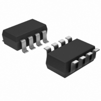
ADG1219BRJZ-REEL7 Analog Devices Inc, ADG1219BRJZ-REEL7 Datasheet - Page 12

ADG1219BRJZ-REEL7
Manufacturer Part Number
ADG1219BRJZ-REEL7
Description
IC,ANALOG SWITCH,SINGLE,SPDT,CMOS,TSSOP,8PIN,PLASTIC
Manufacturer
Analog Devices Inc
Series
iCMOS®r
Type
Analog Switchr
Datasheet
1.ADG1219BRJZ-REEL7.pdf
(16 pages)
Specifications of ADG1219BRJZ-REEL7
Function
Switch
Circuit
1 x SPDT
On-state Resistance
270 Ohm
Voltage Supply Source
Single Supply
Voltage - Supply, Single/dual (±)
12 V ~ 15 V
Current - Supply
1µA
Operating Temperature
-40°C ~ 85°C
Mounting Type
Surface Mount
Package / Case
SOT-23-8
Multiplexer Configuration
Single SPDT
Number Of Inputs
1
Number Of Outputs
2
Number Of Channels
1
Analog Switch On Resistance
475@10.8VOhm
Package Type
SOT-23
Power Supply Requirement
Single/Dual
Single Supply Voltage (typ)
12V
Dual Supply Voltage (typ)
±15V
Mounting
Surface Mount
Pin Count
8
Operating Temp Range
-40C to 125C
Operating Temperature Classification
Automotive
Package
8SOT-23
Maximum On Resistance
475@10.8V Ohm
Maximum Propagation Delay Bus To Bus
170@±15V|250@12V ns
Maximum High Level Output Current
30 mA
Maximum Turn-off Time
185@12V ns
Maximum Turn-on Time
150@12V ns
Switch Architecture
SPDT
Power Supply Type
Single|Dual
Lead Free Status / RoHS Status
Lead free / RoHS Compliant
Lead Free Status / RoHS Status
Lead free / RoHS Compliant
Other names
ADG1219BRJZ-REEL7TR
Available stocks
Company
Part Number
Manufacturer
Quantity
Price
Company:
Part Number:
ADG1219BRJZ-REEL7
Manufacturer:
Allegro
Quantity:
48 573
ADG1219
TEST CIRCUITS
V
IN
IN
0.1µF
V
V
DD
DD
V
S
V
SA
GND
S
NC
I
V
OFF ISOLATION = 20 log
S
V
SS
SS
(OFF)
A
SB
NC = NO CONNECT
Figure 23. On Resistance
S
Figure 24. Off Leakage
Figure 26. Off Isolation
Figure 25. On Leakage
0.1µF
S
S
V
50Ω
NC
D
D
D
I
V
D
V
OUT
I
(ON)
A
V
S
D
D
(OFF)
A
V
D
R
50Ω
ANALYZER
NETWORK
L
I
50Ω
DS
V
OUT
V
S
Rev. A | Page 12 of 16
V
V
IN
IN
IN
CHANNEL-TO-CHANNEL CROSSTALK = 20 log
IN
V
0.1µF
0.1µF
OUT
INSERTION LOSS = 20 log
ANALYZER
NETWORK
V
V
V
V
DD
DD
DD
DD
V
SA
GND
GND
Figure 27. Channel-to-Channel Crosstalk
S
S
R
50Ω
L
D
V
V
V
V
SS
SS
SS
SS
SB
Figure 29. THD + Noise
0.1µF
0.1µF
Figure 28. Bandwidth
50Ω
V
NC
OUT
V
IN
OUT
WITHOUT SWITCH
0.1µF
WITH SWITCH
SA
SB
R
10kΩ
L
V
V
DD
DD
GND
V
AUDIO PRECISION
V
OUT
V
S
R
50Ω
OUT
ANALYZER
V
NETWORK
L
V
50Ω
SS
R
SS
S
V p-p
V
D
0.1µF
OUT
V
V
S
S
R
50Ω


