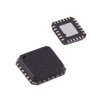
ADF4360-6BCPZ Analog Devices Inc, ADF4360-6BCPZ Datasheet - Page 6

ADF4360-6BCPZ
Manufacturer Part Number
ADF4360-6BCPZ
Description
IC,FREQUENCY SYNTHESIZER,BICMOS,LLCC,24PIN,PLASTIC
Manufacturer
Analog Devices Inc
Type
Fanout Distribution, Integer N Synthesizer (RF)r
Datasheet
1.ADF4360-6BCPZRL.pdf
(24 pages)
Specifications of ADF4360-6BCPZ
Pll
Yes
Input
CMOS
Output
Clock
Number Of Circuits
1
Ratio - Input:output
1:2
Differential - Input:output
No/No
Frequency - Max
1.25GHz
Divider/multiplier
Yes/No
Voltage - Supply
3 V ~ 3.6 V
Operating Temperature
-40°C ~ 85°C
Mounting Type
Surface Mount
Package / Case
24-LFCSP
Frequency-max
1.25GHz
Number Of Elements
1
Pll Input Freq (min)
10MHz
Pll Input Freq (max)
250MHz
Operating Supply Voltage (typ)
3.3V
Operating Temp Range
-40C to 85C
Package Type
LFCSP EP
Output Frequency Range
1050 to 1250MHz
Operating Supply Voltage (min)
3V
Operating Supply Voltage (max)
3.6V
Operating Temperature Classification
Industrial
Pin Count
24
Lead Free Status / RoHS Status
Lead free / RoHS Compliant
For Use With
EVAL-ADF4360-6EBZ1 - BOARD EVALUATION FOR ADF4360-6
Lead Free Status / Rohs Status
Compliant
Available stocks
Company
Part Number
Manufacturer
Quantity
Price
Company:
Part Number:
ADF4360-6BCPZ
Manufacturer:
Analog Devices Inc
Quantity:
135
Company:
Part Number:
ADF4360-6BCPZ
Manufacturer:
AD
Quantity:
724
Part Number:
ADF4360-6BCPZ
Manufacturer:
ADI/亚德诺
Quantity:
20 000
ADF4360-6
ABSOLUTE MAXIMUM RATINGS
T
Table 3.
Parameter
AV
AV
V
V
Digital I/O Voltage to GND
Analog I/O Voltage to GND
REF
Operating Temperature Range
CSP θ
Lead Temperature, Soldering
1
ESD CAUTION
ESD (electrostatic discharge) sensitive device. Electrostatic charges as high as 4000 V readily accumulate
on the human body and test equipment and can discharge without detection. Although this product features
proprietary ESD protection circuitry, permanent damage may occur on devices subjected to high energy elec-
trostatic discharges. Therefore, proper ESD precautions are recommended to avoid performance degradation
or loss of functionality.
GND = AGND = DGND = 0 V.
VCO
VCO
A
Maximum Junction Temperature
(Paddle Soldered)
(Paddle Not Soldered)
Vapor Phase (60 sec)
Infrared (15 sec)
DD
DD
= 25°C, unless otherwise noted.
IN
to GND
to AV
to GND
to DV
to GND
JA
Thermal Impedance
DD
DD
1
Rating
−0.3 V to +3.9 V
−0.3 V to +0.3 V
−0.3 V to +3.9 V
−0.3 V to +0.3 V
−0.3 V to V
−0.3 V to V
−0.3 V to V
150°C
50°C/W
88°C/W
215°C
220°C
DD
DD
DD
+ 0.3 V
+ 0.3 V
+ 0.3 V
Rev. A | Page 6 of 24
Stresses above those listed under Absolute Maximum Ratings
may cause permanent damage to the device. This is a stress rat-
ing only; functional operation of the device at these or any
other conditions above those indicated in the operational sec-
tions of this specification is not implied. Exposure to absolute
maximum rating conditions for extended periods may affect
device reliability.
This device is a high performance RF integrated circuit with an
ESD rating of <1 kV and it is ESD sensitive. Proper precautions
should be taken for handling and assembly.
TRANSISTOR COUNT
12543 (CMOS) and 700 (Bipolar).


