ADCMP605BCPZ-WP Analog Devices Inc, ADCMP605BCPZ-WP Datasheet - Page 5
ADCMP605BCPZ-WP
Manufacturer Part Number
ADCMP605BCPZ-WP
Description
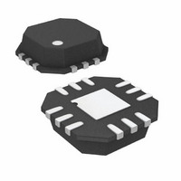
IC,VOLT COMPARATOR,SINGLE,LLCC,12PIN,PLASTIC
Manufacturer
Analog Devices Inc
Type
with Latchr
Datasheet
1.ADCMP604BKSZ-REEL7.pdf
(16 pages)
Specifications of ADCMP605BCPZ-WP
Number Of Elements
1
Output Type
Complementary, LVDS, Rail-to-Rail
Voltage - Supply
2.5 V ~ 5.5 V, ±1.25 V ~ 2.75 V
Mounting Type
Surface Mount
Package / Case
12-VFQFN, CSP Exposed Pad
No. Of Comparators
1
Ic Output Type
LVDS
Supply Current
1.6mA
Supply Voltage Range
2.5V To 5.5V
Amplifier Case Style
LFCSP
No. Of Pins
12
Operating Temperature Range
-40°C To +125°C
Lead Free Status / RoHS Status
Lead free / RoHS Compliant
Available stocks
Company
Part Number
Manufacturer
Quantity
Price
Company:

Part Number:
ADCMP605BCPZ-WP
Manufacturer:
SANYO
Quantity:
12 000
Part Number:
ADCMP605BCPZ-WP
Manufacturer:
ADI/亚德诺
Quantity:
20 000


TIMING INFORMATION
Figure 2 illustrates the ADCMP604/ADCMP605 latch timing relationships. Table 2 provides definitions of the terms shown in Figure 2.
Table 2. Timing Descriptions
Symbol
t
t
t
t
t
t
t
t
t
V
PDH
PDL
PLOH
PLOL
H
PL
S
R
F
OD
Timing
Input-to-Output High Delay
Input-to-Output Low Delay
Latch Enable-to-Output High Delay
Latch Enable-to-Output Low Delay
Minimum Hold Time
Minimum Latch Enable Pulse Width
Minimum Setup Time
Output Rise Time
Output Fall Time
Voltage Overdrive
INPUT VOLTAGE
LATCH ENABLE
DIFFERENTIAL
Q OUTPUT
Q OUTPUT
V
IN
Description
Propagation delay measured from the time the input signal crosses the reference (± the
input offset voltage) to the 50% point of an output low-to-high transition.
Propagation delay measured from the time the input signal crosses the reference (± the
input offset voltage) to the 50% point of an output high-to-low transition.
Propagation delay measured from the 50% point of the latch enable signal low-to-high
transition to the 50% point of an output low-to-high transition.
Propagation delay measured from the 50% point of the latch enable signal low-to-high
transition to the 50% point of an output high-to-low transition.
Minimum time after the negative transition of the latch enable signal that the input
signal must remain unchanged to be acquired and held at the outputs.
Minimum time that the latch enable signal must be high to acquire an input signal change.
Minimum time before the negative transition of the latch enable signal occurs that an
input signal change must be present to be acquired and held at the outputs.
Amount of time required to transition from a low to a high output as measured at the
20% and 80% points.
Amount of time required to transition from a high to a low output as measured at the
20% and 80% points.
Difference between the input voltages, V
Figure 2. System Timing Diagram
V
t
S
OD
t
t
Rev. A | Page 5 of 16
PDL
PDH
t
H
t
R
t
F
t
PL
t
t
PLOH
PLOL
A
and V
B
.
B
ADCMP604/ADCMP605
1.1V
V
50%
50%
N
± V
OS
Related parts for ADCMP605BCPZ-WP
Image
Part Number
Description
Manufacturer
Datasheet
Request
R

Part Number:
Description:
±1.7g Dual-Axis IMEMS Accelerometer Evaluation Board
Manufacturer:
Analog Devices Inc
Datasheet:

Part Number:
Description:
Inertial Sensor Evaluation System
Manufacturer:
Analog Devices Inc
Datasheet:
Part Number:
Description:
Manufacturer:
Analog Devices Inc
Datasheet:
Part Number:
Description:
Manufacturer:
Analog Devices Inc
Datasheet:
Part Number:
Description:
Manufacturer:
Analog Devices Inc
Datasheet:
Part Number:
Description:
Manufacturer:
Analog Devices Inc
Datasheet:
Part Number:
Description:
Manufacturer:
Analog Devices Inc
Datasheet:
Part Number:
Description:
Manufacturer:
Analog Devices Inc
Datasheet:
Part Number:
Description:
Manufacturer:
Analog Devices Inc
Datasheet:
Part Number:
Description:
Manufacturer:
Analog Devices Inc
Datasheet:
Part Number:
Description:
Manufacturer:
Analog Devices Inc
Datasheet:
Part Number:
Description:
Manufacturer:
Analog Devices Inc
Datasheet:
Part Number:
Description:
Manufacturer:
Analog Devices Inc
Datasheet: