ADCMP605BCPZ-WP Analog Devices Inc, ADCMP605BCPZ-WP Datasheet - Page 11
ADCMP605BCPZ-WP
Manufacturer Part Number
ADCMP605BCPZ-WP
Description
IC,VOLT COMPARATOR,SINGLE,LLCC,12PIN,PLASTIC
Manufacturer
Analog Devices Inc
Type
with Latchr
Datasheet
1.ADCMP604BKSZ-REEL7.pdf
(16 pages)
Specifications of ADCMP605BCPZ-WP
Number Of Elements
1
Output Type
Complementary, LVDS, Rail-to-Rail
Voltage - Supply
2.5 V ~ 5.5 V, ±1.25 V ~ 2.75 V
Mounting Type
Surface Mount
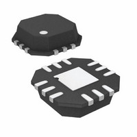
Package / Case
12-VFQFN, CSP Exposed Pad
No. Of Comparators
1
Ic Output Type
LVDS
Supply Current
1.6mA
Supply Voltage Range
2.5V To 5.5V
Amplifier Case Style
LFCSP
No. Of Pins
12
Operating Temperature Range
-40°C To +125°C
Lead Free Status / RoHS Status
Lead free / RoHS Compliant
Available stocks
Company
Part Number
Manufacturer
Quantity
Price
Company:

Part Number:
ADCMP605BCPZ-WP
Manufacturer:
SANYO
Quantity:
12 000
Part Number:
ADCMP605BCPZ-WP
Manufacturer:
ADI/亚德诺
Quantity:
20 000


COMPARATOR PROPAGATION DELAY
DISPERSION
The ADCMP604/ADCMP605 comparators are designed to
reduce propagation delay dispersion over a wide input overdrive
range of 5 mV to V
variation in propagation delay that results from a change in the
degree of overdrive or slew rate (how far or how fast the input
signal is driven past the switching threshold).
Propagation delay dispersion is a specification that becomes
important in high speed, time-critical applications, such as data
communications, automatic test and measurement, and instru-
mentation. It is also important in event-driven applications, such
as pulse spectroscopy, nuclear instrumentation, and medical
imaging. Dispersion is defined as the variation in propagation
delay as the input overdrive conditions are changed (see Figure 17
and Figure 18).
The ADCMP604/ADCMP605 dispersion is typically <1.6 ns as
the overdrive varies from 10 mV to 125 mV. This specification
applies to both positive and negative signals because each of
the ADCMP604 and ADCMP605 has substantially equal delays
for positive-going and negative-going inputs and very low
output skews.
INPUT VOLTAGE
INPUT VOLTAGE
Q/Q OUTPUT
Q/Q OUTPUT
Figure 17. Propagation Delay—Overdrive Dispersion
Figure 18. Propagation Delay—Slew Rate Dispersion
CCI
− 1 V. Propagation delay dispersion is the
10V/ns
1V/ns
500mV OVERDRIVE
10mV OVERDRIVE
DISPERSION
DISPERSION
V
V
N
N
± V
± V
OS
OS
Rev. A | Page 11 of 16
COMPARATOR HYSTERESIS
The addition of hysteresis to a comparator is often desirable in a
noisy environment, or when the differential input amplitudes
are relatively small or slow moving. The transfer function for a
comparator with hysteresis is shown in Figure 19. As the input
voltage approaches the threshold (0 V, in this example) from
below the threshold region in a positive direction, the comparator
switches from low to high when the input crosses +V
new switching threshold becomes −V
in the high state until the threshold, −V
below the threshold region in a negative direction. In this manner,
noise or feedback output signals centered on 0 V input cannot
cause the comparator to switch states unless it exceeds the region
bounded by ±V
The customary technique for introducing hysteresis into a
comparator uses positive feedback from the output back to
the input. One limitation of this approach is that the amount
of hysteresis varies with the output logic levels, resulting in
hysteresis that is not symmetric about the threshold. The
external feedback network can also introduce significant
parasitics that reduce high speed performance and induce
oscillation in some cases.
The ADCMP605 comparator offers a programmable hysteresis
feature that significantly improves accuracy and stability.
Connecting an external pull-down resistor or a current source
from the LE/HYS pin to GND varies the amount of hysteresis
in a predictable and stable manner. Leaving the LE/HYS
pin disconnected or driving it high removes hysteresis. The
maximum hysteresis that can be applied using this pin is
approximately 160 mV. Figure 20 illustrates the amount of
hysteresis applied as a function of external resistor value. Figure 11
illustrates hysteresis as a function of current.
Figure 19. Comparator Hysteresis Transfer Function
H
/2.
–V
2
H
OUTPUT
V
OL
0V
ADCMP604/ADCMP605
V
OH
H
/2. The comparator remains
+V
H
2
/2, is crossed from
H
INPUT
H
/2. The
Related parts for ADCMP605BCPZ-WP
Image
Part Number
Description
Manufacturer
Datasheet
Request
R

Part Number:
Description:
±1.7g Dual-Axis IMEMS Accelerometer Evaluation Board
Manufacturer:
Analog Devices Inc
Datasheet:

Part Number:
Description:
Inertial Sensor Evaluation System
Manufacturer:
Analog Devices Inc
Datasheet:
Part Number:
Description:
Manufacturer:
Analog Devices Inc
Datasheet:
Part Number:
Description:
Manufacturer:
Analog Devices Inc
Datasheet:
Part Number:
Description:
Manufacturer:
Analog Devices Inc
Datasheet:
Part Number:
Description:
Manufacturer:
Analog Devices Inc
Datasheet:
Part Number:
Description:
Manufacturer:
Analog Devices Inc
Datasheet:
Part Number:
Description:
Manufacturer:
Analog Devices Inc
Datasheet:
Part Number:
Description:
Manufacturer:
Analog Devices Inc
Datasheet:
Part Number:
Description:
Manufacturer:
Analog Devices Inc
Datasheet:
Part Number:
Description:
Manufacturer:
Analog Devices Inc
Datasheet:
Part Number:
Description:
Manufacturer:
Analog Devices Inc
Datasheet:
Part Number:
Description:
Manufacturer:
Analog Devices Inc
Datasheet: