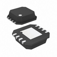
ADA4941-1YCPZ-RL Analog Devices Inc, ADA4941-1YCPZ-RL Datasheet - Page 22

ADA4941-1YCPZ-RL
Manufacturer Part Number
ADA4941-1YCPZ-RL
Description
Amplifier, Other
Manufacturer
Analog Devices Inc
Type
ADC Driverr
Datasheet
1.ADA4941-1YCPZ-R7.pdf
(24 pages)
Specifications of ADA4941-1YCPZ-RL
Design Resources
Converting a Single-Ended Signal with AD7982 Differential PulSAR ADC (CN0032) Converting a Single-Ended Signal with AD7984 Differential PulSAR ADC (CN0033)
Applications
Data Acquisition
Mounting Type
Surface Mount
Package / Case
8-LFCSP
Number Of Channels
1
Number Of Elements
2
Power Supply Requirement
Single
Common Mode Rejection Ratio
84dB
Voltage Gain Db
6.06dB
Unity Gain Bandwidth Product (typ)
31MHz
Input Resistance
24@5VMohm
Input Offset Voltage
0.4@5VmV
Input Bias Current
4.5@5VnA
Single Supply Voltage (typ)
3/5/9V
Dual Supply Voltage (typ)
Not RequiredV
Power Supply Rejection Ratio
87dB
Rail/rail I/o Type
Rail to Rail Output
Single Supply Voltage (min)
2.7V
Single Supply Voltage (max)
12V
Dual Supply Voltage (min)
Not RequiredV
Dual Supply Voltage (max)
Not RequiredV
Operating Temp Range
-40C to 125C
Operating Temperature Classification
Automotive
Mounting
Surface Mount
Pin Count
8
Package Type
LFCSP EP
Lead Free Status / RoHS Status
Lead free / RoHS Compliant
Lead Free Status / RoHS Status
Lead free / RoHS Compliant
ADA4941-1
DRIVING THE AD7687 ADC
The ADA4941-1 is an excellent driver for high resolution
ADCs, such as the AD7687, as shown in Figure 56. The Sallen-
Key, low-pass filter shown in Figure 54 is included in this
example but is not required. The circuit shown in Figure 56
accepts single-ended input signals that swing between 0 V and 3 V.
The
buffered by one of the
AD7687
of 6 V. The reference voltage is also divided by two and buffered
to supply the midsupply REF level of 1.5 V for the ADA4941-1.
ADR443
REF input, providing a differential input full-scale level
+5V
10µF
provides a stable, low noise, 3 V reference that is
0.1µF
AD8032
VIN
0V TO 3V
2
562Ω
V
IN
amplifiers and applied to the
ADR443
GND
4
3.9nF
562Ω
V
OUT
10nF
6
562Ω
VIN
1kΩ
R
G
0.1µF
1.69kΩ
Figure 56. ADA4941-1 Driving the AD7687 ADC
500Ω
560pF
3
2
1
8
Figure 57. Gain of −2 Configuration
1
8
8
4
FB
IN
FB
IN
AD8032
+5V
6
–5V
1kΩ
6
–5V
1/2
R
Rev. B | Page 22 of 24
0.1µF
F
3
A1
3
A1
1
V
V
V
V
+5V
+5V
S+
S–
S+
S–
2
2
ADA4941-1
REF
REF
10µF
500Ω
1kΩ
500Ω
10µF
1kΩ
GAIN OF −2 CONFIGURATION
The ADA4941-1 can be operated in a configuration referred
to as gain of −2. Clearly, a gain of −2 can be achieved by
simply swapping the outputs of a gain of +2 circuit, but the
configuration described here is different. The configuration is
referred to as having negative gain to emphasize that the input
amplifier, A1, is operated as an inverting amplifier instead of in
its usual noninverting mode. As implied in its name, the voltage
gain from VIN to V
of −2 configuration on ±5 V supplies.
The gain of −2 configuration is most useful in applications that
have wide input swings because the input common-mode
voltages are held at constant levels. The signal size is therefore
constrained by the output swing limits. The gain of −2 has a low
input resistance that is equal to R
1kΩ
1kΩ
1kΩ
A2
1kΩ
A2
0.1µF
0.1µF
5
6
OUT+
OUT–
V
AD8032
O, dm
OUT+
OUT–
+
–
1/2
4
5
O
7
, dm is −2 V/V. See Figure 57 for the gain
4
5
33Ω
33Ω
2.7nF
2.7nF
G
.
3
4
0.1µF
IN+
IN–
AD7687
VDD
GND
5
2
REF
1


