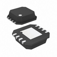
ADA4941-1YCPZ-RL Analog Devices Inc, ADA4941-1YCPZ-RL Datasheet - Page 16

ADA4941-1YCPZ-RL
Manufacturer Part Number
ADA4941-1YCPZ-RL
Description
Amplifier, Other
Manufacturer
Analog Devices Inc
Type
ADC Driverr
Datasheet
1.ADA4941-1YCPZ-R7.pdf
(24 pages)
Specifications of ADA4941-1YCPZ-RL
Design Resources
Converting a Single-Ended Signal with AD7982 Differential PulSAR ADC (CN0032) Converting a Single-Ended Signal with AD7984 Differential PulSAR ADC (CN0033)
Applications
Data Acquisition
Mounting Type
Surface Mount
Package / Case
8-LFCSP
Number Of Channels
1
Number Of Elements
2
Power Supply Requirement
Single
Common Mode Rejection Ratio
84dB
Voltage Gain Db
6.06dB
Unity Gain Bandwidth Product (typ)
31MHz
Input Resistance
24@5VMohm
Input Offset Voltage
0.4@5VmV
Input Bias Current
4.5@5VnA
Single Supply Voltage (typ)
3/5/9V
Dual Supply Voltage (typ)
Not RequiredV
Power Supply Rejection Ratio
87dB
Rail/rail I/o Type
Rail to Rail Output
Single Supply Voltage (min)
2.7V
Single Supply Voltage (max)
12V
Dual Supply Voltage (min)
Not RequiredV
Dual Supply Voltage (max)
Not RequiredV
Operating Temp Range
-40C to 125C
Operating Temperature Classification
Automotive
Mounting
Surface Mount
Pin Count
8
Package Type
LFCSP EP
Lead Free Status / RoHS Status
Lead free / RoHS Compliant
Lead Free Status / RoHS Status
Lead free / RoHS Compliant
ADA4941-1
In this case, the linear output voltage is limited by A1. On the
low end, the output of A1 starts to saturate and show degraded
linearity when VOP approaches 200 mV. On the high end, the
input of A1 becomes saturated and exhibits degraded linearity
when VIN moves beyond 4 V (within 1 V of VCC). This limits
the linear differential output voltage in the circuit shown in
Figure 49 to about 7.6 V p-p.
Figure 50 shows a single 5 V supply connection for G = 5. The
R
the REF input provides a centered 2.5 V output common-mode
voltage. The transfer function is then
The output range limits of A1 and A2 limit the differential
output voltage of the circuit shown in Figure 50 to approximately
8.4 V p-p.
DC ERROR CALCULATIONS
Figure 51 shows the major contributions to the dc output
voltage error. For each output, the total error voltage can be
calculated using familiar op amp concepts. Equation 9 expresses
the dc voltage error present at the VOP output.
R
F
G
and R
Figure 50. 5 V Supply, G = 5, Single-Ended-to-Differential Amplifier
VOP − VON = 5( VIN ) − 5 V
R
VOP_error
⎛
⎜
⎜
⎝
S–
1
665Ω
+
IN
G
R
R
network sets the gain of A1 to 2.5, and the 2.5 V at
R
G
F
V
F
I
I
OS–
⎞
⎟
⎟
⎠
BN–
BP–
[
V
402Ω
A1
VIN
A1
A1
OS
1
8
=
1
8
_A1
FB
IN
FB
IN
1.02kΩ
Figure 51. DC Error Sources
6
−
R
A1
3
A1
S–
(
I
V
V
REF
+5V
BP
S+
S–
2
2
_A1
REF
REF
+2.5V
)(
I
I
BN–
BP–
500Ω
500Ω
1kΩ
R
1kΩ
A2
A2
S
_IN
V
)
OS–
]
1kΩ
A2
+
A2
(
I
BP
1kΩ
A2
_A1
OUT+
OUT–
)
VOP
VON
R
+
–
+
–
OUT+
OUT–
F
4
5
VOP
VON
+
–
+
–
Rev. B | Page 16 of 24
4
5
(8)
(9)
When using data from the Specifications tables, it is often more
expedient to use input offset current in place of the individual
input bias currents when calculating errors. Input offset current
is defined as the magnitude of the difference between the two
input bias currents. Using this definition, each input bias
current can be expressed in terms of the average of the two
input bias currents, I
I
this case, Equation 9 is reduced to
Equation 10 expresses the dc voltage error present at the VON
output.
The internal 500 Ω resistor is provided on-chip to minimize dc
errors due to the input offset current in A2. The minimum
error is achieved when R
is reduced to
The differential output voltage error V
difference between VOP_error and VON_error:
The output offset voltage of each amplifier in the ADA4941-1
also includes the effects of finite common-mode rejection ratio
(CMRR), power supply rejection ratio (PSRR), and dc open-
loop gain (A
where:
V
the effects of CMRR, PSRR, and A
Δ indicates the change in conditions from nominal.
V
IN, and for A2, the voltage at REF).
V
VOUT is either op amp output.
BP, N
OS
CM
S
is the power supply voltage.
_nom is the nominal output offset voltage without including
= I
is the input common-mode voltage (for A1, the voltage at
VON_error = −( VOP_error ) + 2[ V
( I
VON_error =
−( VOP_error ) + 2[ V
V
VOP_error
V
BP
O
OS
B
_error, dm = VOP_error − VON_error
_A2 )( R
± I
=
V
OS
VOL
OS
/2. DC errors are minimized when R
_nom
).
S
_REF + 500)] + 1000( I
=
⎛
⎜
⎜
⎝
1
B
+
+
, and the input offset current, I
R
CMRR
R
Δ
G
F
S
V
OS
_REF = 0 Ω. In this case, Equation 10
⎞
⎟
⎟
⎠
CM
_A2 ] + ( I
[
V
OS
+
_A1
PSRR
Δ
VOL
V
]
OS
+
S
.
)1000
(
O
BN
+
I
OS
_error, dm, is the
OS
_A2 )
Δ
_A2 −
)
VOUT
A
R
VOL
F
(
( R
R
S
S
S
= R
_REF = 0 Ω)
=
OS
, as
R
F
F
|| R
||
R
G
(10)
(11)
(12)
G
. In
)


