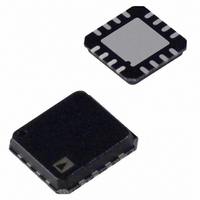
ADA4939-1YCPZ-R7 Analog Devices Inc, ADA4939-1YCPZ-R7 Datasheet - Page 8

ADA4939-1YCPZ-R7
Manufacturer Part Number
ADA4939-1YCPZ-R7
Description
IC,Differential Amplifier,SINGLE,BIPOLAR,LLCC,16PIN,PLASTIC
Manufacturer
Analog Devices Inc
Type
Differential ADC Driverr
Datasheet
1.ADA4939-1YCPZ-R7.pdf
(24 pages)
Specifications of ADA4939-1YCPZ-R7
Amplifier Type
Differential
Number Of Circuits
1
Output Type
Differential
Slew Rate
6800 V/µs
-3db Bandwidth
1.4GHz
Current - Input Bias
10µA
Voltage - Input Offset
500µV
Current - Supply
36.5mA
Current - Output / Channel
100mA
Voltage - Supply, Single/dual (±)
3 V ~ 5.25 V, ±1.5 V ~ 2.625 V
Operating Temperature
-40°C ~ 105°C
Mounting Type
Surface Mount
Package / Case
16-LFCSP
Number Of Channels
1
Number Of Elements
1
Power Supply Requirement
Single
Common Mode Rejection Ratio
77dB
Input Resistance
0.45MOhm
Input Offset Voltage
2.8mV
Input Bias Current
2.2uA
Single Supply Voltage (typ)
5V
Dual Supply Voltage (typ)
Not RequiredV
Power Supply Rejection Ratio
80dB
Rail/rail I/o Type
No
Single Supply Voltage (min)
3V
Single Supply Voltage (max)
5.25V
Dual Supply Voltage (min)
Not RequiredV
Dual Supply Voltage (max)
Not RequiredV
Operating Temp Range
-40C to 105C
Operating Temperature Classification
Industrial
Mounting
Surface Mount
Pin Count
16
Package Type
LFCSP EP
Lead Free Status / RoHS Status
Lead free / RoHS Compliant
Gain Bandwidth Product
-
Lead Free Status / Rohs Status
Compliant
Other names
ADA4939-1YCPZ-R7TR
Available stocks
Company
Part Number
Manufacturer
Quantity
Price
Company:
Part Number:
ADA4939-1YCPZ-R7
Manufacturer:
Analog Devices Inc
Quantity:
1 948
ADA4939-1/ADA4939-2
PIN CONFIGURATIONS AND FUNCTION DESCRIPTIONS
Table 9. ADA4939-1 Pin Function Descriptions
Pin No.
1
2
3
4
5 to 8
9
10
11
12
13 to 16
Table 10. ADA4939-2 Pin Function Descriptions
Pin No.
1
2
3, 4
5
6
7
8
9, 10
11
12
13
14
15, 16
17
18
19
20
21, 22
23
24
Figure 5. ADA4939-1 Pin Configuration
–FB
+FB
+IN
–IN
1
2
3
4
Mnemonic
−FB
+IN
−IN
+FB
+V
V
+OUT
−OUT
PD
−V
Mnemonic
−IN1
+FB1
+V
−FB2
+IN2
−IN2
+FB2
+V
V
+OUT2
−OUT2
PD2
−V
V
+OUT1
−OUT1
PD1
−V
−FB1
+IN1
ADA4939-1
(Not to Scale)
OCM
OCM2
OCM1
TOP VIEW
S
S
S1
S2
S2
S1
PIN 1
INDICATOR
12 PD
11 –OUT
10 +OUT
9 V
OCM
Description
Negative Input Summing Node 1
Positive Output Feedback 1
Positive Supply Voltage 1
Negative Output Feedback 2
Positive Input Summing Node 2
Negative Input Summing Node 2
Positive Output Feedback 2
Positive Supply Voltage 2
Output Common-Mode Voltage 2
Positive Output 2
Negative Output 2
Power-Down Pin 2
Negative Supply Voltage 2
Output Common-Mode Voltage 1
Positive Output 1
Negative Output 1
Power-Down Pin 1
Negative Supply Voltage 1
Negative Output Feedback 1
Positive Input Summing Node 1
Description
Negative Output for Feedback Component Connection
Positive Input Summing Node
Negative Input Summing Node
Positive Output for Feedback Component Connection
Positive Supply Voltage
Output Common-Mode Voltage
Positive Output for Load Connection
Negative Output for Load Connection
Power-Down Pin
Negative Supply Voltage
Rev. 0 | Page 8 of 24
+FB1
–FB2
+V
+V
+IN2
–IN1
Figure 6. ADA4939-2 Pin Configuration
S1
S1
1
2
3
4
5
6
ADA4939-2
(Not to Scale)
TOP VIEW
PIN 1
INDICATOR
18
17
16
15
14
13
–V
+OUT1
V
–V
PD2
–OUT2
OCM1
S2
S2


