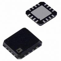
ADA4939-1YCPZ-R7 Analog Devices Inc, ADA4939-1YCPZ-R7 Datasheet - Page 22

ADA4939-1YCPZ-R7
Manufacturer Part Number
ADA4939-1YCPZ-R7
Description
IC,Differential Amplifier,SINGLE,BIPOLAR,LLCC,16PIN,PLASTIC
Manufacturer
Analog Devices Inc
Type
Differential ADC Driverr
Datasheet
1.ADA4939-1YCPZ-R7.pdf
(24 pages)
Specifications of ADA4939-1YCPZ-R7
Amplifier Type
Differential
Number Of Circuits
1
Output Type
Differential
Slew Rate
6800 V/µs
-3db Bandwidth
1.4GHz
Current - Input Bias
10µA
Voltage - Input Offset
500µV
Current - Supply
36.5mA
Current - Output / Channel
100mA
Voltage - Supply, Single/dual (±)
3 V ~ 5.25 V, ±1.5 V ~ 2.625 V
Operating Temperature
-40°C ~ 105°C
Mounting Type
Surface Mount
Package / Case
16-LFCSP
Number Of Channels
1
Number Of Elements
1
Power Supply Requirement
Single
Common Mode Rejection Ratio
77dB
Input Resistance
0.45MOhm
Input Offset Voltage
2.8mV
Input Bias Current
2.2uA
Single Supply Voltage (typ)
5V
Dual Supply Voltage (typ)
Not RequiredV
Power Supply Rejection Ratio
80dB
Rail/rail I/o Type
No
Single Supply Voltage (min)
3V
Single Supply Voltage (max)
5.25V
Dual Supply Voltage (min)
Not RequiredV
Dual Supply Voltage (max)
Not RequiredV
Operating Temp Range
-40C to 105C
Operating Temperature Classification
Industrial
Mounting
Surface Mount
Pin Count
16
Package Type
LFCSP EP
Lead Free Status / RoHS Status
Lead free / RoHS Compliant
Gain Bandwidth Product
-
Lead Free Status / Rohs Status
Compliant
Other names
ADA4939-1YCPZ-R7TR
Available stocks
Company
Part Number
Manufacturer
Quantity
Price
Company:
Part Number:
ADA4939-1YCPZ-R7
Manufacturer:
Analog Devices Inc
Quantity:
1 948
ADA4939-1/ADA4939-2
LAYOUT, GROUNDING, AND BYPASSING
As a high speed device, the ADA4939 is sensitive to the
PCB environment in which it operates. Realizing its superior
performance requires attention to the details of high speed
PCB design. This section shows a detailed example of how the
ADA4939-1 was addressed.
The first requirement is a solid ground plane that covers as
much of the board area around the ADA4939-1 as possible.
However, the area near the feedback resistors (R
(R
cleared of all ground and power planes (see Figure 51). Clearing
the ground and power planes minimizes any stray capacitance at
these nodes and prevents peaking of the response of the amplifier
at high frequencies.
The thermal resistance, θ
the exposed pad, soldered to a high thermal conductivity four-layer
circuit board, as described in EIA/JESD 51-7.
G
), and the input summing nodes (Pin 2 and Pin 3) should be
Figure 51. Ground and Power Plane Voiding in Vicinity of R
Figure 53. Cross-Section of Four-Layer PCB Showing Thermal Via Connection to Buried Ground Plane (Dimensions in Millimeters)
JA
, is specified for the device, including
GROUND PLANE
BOTTOM METAL
POWER PLANE
TOP METAL
F
), gain resistors
F
and R
G
Rev. 0 | Page 22 of 24
VIA HOLE
PLATED
1.30
0.30
The power supply pins should be bypassed as close to the device
as possible and directly to a nearby ground plane. High frequency
ceramic chip capacitors should be used. It is recommended that
two parallel bypass capacitors (1000 pF and 0.1 μF) be used for
each supply. The 1000 pF capacitor should be placed closer to
the device. Further away, low frequency bypassing should be
provided, using 10 μF tantalum capacitors from each supply
to ground.
Signal routing should be short and direct to avoid parasitic
effects. Wherever complementary signals exist, a symmetrical
layout should be provided to maximize balanced performance.
When routing differential signals over a long distance, PCB
traces should be close together, and any differential wiring
should be twisted such that loop area is minimized. Doing this
reduces radiated energy and makes the circuit less susceptible
to interference.
Figure 52. Recommended PCB Thermal Attach Pad Dimensions (Millimeters)
1.30
0.80
1.30
0.80


