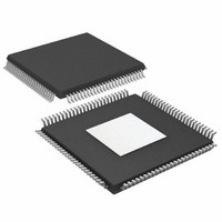
AD9776ABSVZRL Analog Devices Inc, AD9776ABSVZRL Datasheet - Page 33

AD9776ABSVZRL
Manufacturer Part Number
AD9776ABSVZRL
Description
IC,D/A CONVERTER,DUAL,12-BIT,CMOS,TQFP,100PIN
Manufacturer
Analog Devices Inc
Datasheet
1.AD9776ABSVZ.pdf
(60 pages)
Specifications of AD9776ABSVZRL
Number Of Bits
12
Data Interface
Parallel
Number Of Converters
2
Voltage Supply Source
Analog and Digital
Power Dissipation (max)
300mW
Operating Temperature
-40°C ~ 85°C
Mounting Type
Surface Mount
Package / Case
100-TQFP Exposed Pad, 100-eTQFP, 100-HTQFP, 100-VQFP
Lead Free Status / RoHS Status
Lead free / RoHS Compliant
For Use With
AD9776A-EBZ - BOARD EVALUATION AD9776A
Settling Time
-
Lead Free Status / RoHS Status
Lead free / RoHS Compliant
Available stocks
Company
Part Number
Manufacturer
Quantity
Price
Company:
Part Number:
AD9776ABSVZRL
Manufacturer:
Analog Devices Inc
Quantity:
10 000
Figure 64. Interpolation/Modulation Combination of −f
Figure 66. Interpolation/Modulation Combination of 2f
Figure 65. Interpolation/Modulation Combination of f
–100
–100
–100
–10
–20
–30
–40
–50
–60
–70
–80
–90
–10
–20
–30
–40
–50
–60
–70
–80
–90
–10
–20
–30
–40
–50
–60
–70
–80
–90
10
10
10
0
0
0
–4
–4
–4
–3
–3
–3
–2
–2
–2
f
f
f
OUT
OUT
OUT
–1
–1
–1
(× Input Data Rate)
(× Input Data Rate)
(× Input Data Rate)
0
0
0
1
1
1
2
2
2
DAC
DAC
DAC
3
3
3
/8 Filter
/8 Filter
/8 Filter
4
4
4
Rev. A | Page 33 of 60
Shifted mode filter responses allow the pass band to be centered
around ±0.5 f
the shifted mode response does not affect the center frequency
of the signal. Instead, the pass band of the filter is simply shifted.
For example, use the response shown in Figure 67 and assume
the signal in-band is a complex signal over the bandwidth 3.2 f
to 3.3 f
the pass band becomes centered at 3.5 f
remains at the same place in the spectrum. The shifted mode
capability allows the filter pass band to be placed anywhere in
the DAC Nyquist bandwidth.
The AD9776A/AD9778A/AD9779A are dual DACs with
internal complex modulators built into the interpolating filter
response. In dual channel mode, the devices expect the real and
the imaginary components of a complex signal at Digital Input
Port 1 and Digital Input Port 2 (I and Q, respectively). The DAC
outputs then represent the real and imaginary components of
the input signal, modulated by the complex carrier (f
f
With Register 2, Bit 6 set, the device accepts interleaved data
on Port 1 in the I, Q, I, Q … sequence. Note that in interleaved
mode, the channel data rate at the beginning of the I and the Q
data paths is now half the input data rate because of the inter-
leaving. The maximum input data rate is still subject to the
maximum specification of the device. This limits the synthesis
bandwidth available at the input in interleaved mode.
With Register 0x02, Bit 5 (real mode) set, the Q channel and
the internal I and Q digital modulation are turned off. The
output spectrum at the I DAC then represents the signal at
Digital Input Port 1, interpolated by 1×, 2×, 4×, or 8×.
The general recommendation is that if the desired signal is
within ±0.4 × f
this, the shifted filter mode should be used. In any situation, the
total bandwidth of the signal should be less than 0.8 × f
DAC
/4, or f
Figure 67. Interpolation/Modulation Combination of 3f
–100
–10
–20
–30
–40
–50
–60
–70
–80
–90
DATA
10
0
–4
DAC
. If the shifted mode filter response is then selected,
DATA
/8).
DATA
–3
, ±1.5 f
, use the nonshifted filter mode. Outside of
AD9776A/AD9778A/AD9779A
–2
DATA
f
OUT
, ±2.5 f
–1
(× Input Data Rate)
0
DATA
, and ±3.5 f
1
DATA
. However, the signal
2
DATA
DAC
. Switching to
3
DAC
/8 Filter
DATA
/2,
4
.
DATA


