AD9393BBCZ-80 Analog Devices Inc, AD9393BBCZ-80 Datasheet - Page 6
AD9393BBCZ-80
Manufacturer Part Number
AD9393BBCZ-80
Description
Pb-free Low Power HDMI Rx
Manufacturer
Analog Devices Inc
Datasheet
1.AD9393BBCZ-80.pdf
(40 pages)
Specifications of AD9393BBCZ-80
Applications
Video
Interface
HDMI
Voltage - Supply
3.15 V ~ 3.47 V
Package / Case
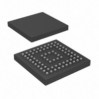
76-CSPBGA
Mounting Type
Surface Mount
Lead Free Status / RoHS Status
Lead free / RoHS Compliant
Available stocks
Company
Part Number
Manufacturer
Quantity
Price
Company:

Part Number:
AD9393BBCZ-80
Manufacturer:
Analog Devices Inc
Quantity:
135
Company:
Part Number:
AD9393BBCZ-80
Manufacturer:
FUJ
Quantity:
1 445
Company:
Part Number:
AD9393BBCZ-80
Manufacturer:
Analog Devices Inc
Quantity:
10 000
Part Number:
AD9393BBCZ-80
Manufacturer:
ADI/亚德诺
Quantity:
20 000


AD9393
PIN CONFIGURATION AND FUNCTION DESCRIPTIONS
Table 4. Complete Pin List
Pin No.
Inputs
Digital Video Data Inputs
Digital Video Clock Inputs
Outputs
B9
K5, K4, K8, K7, J10, K10
K2, K1
B6, A6, B5, A5, B4,
A4, B3, A3, A2, A1,
B1, B2, C1, C2, D1,
D2, E1, E2, F1, F2,
G1, G2, H1, H2
A7
A8
Mnemonic
Rx0+, Rx0−,
Rx1+, Rx1−,
Rx2+, Rx2−
D[23:0]
DCLK
HSOUT
PD
RxC+, RxC−
G
A
B
C
D
E
H
K
F
J
RxC–
GND
D14
D13
D11
D9
D7
D5
D3
D1
1
MCLK
RxC+
D15
D12
D10
D8
D6
D4
D2
D0
2
Description
Power-Down Control. Power-Down Control/Three-State Control. The function
of this pin is programmable via Register 0x26[2:1].
Digital Input Channel x True/Complement. These six pins receive three pairs of
transition minimized differential signaling (TMDS ) pixel data (at 10× the pixel
rate) from a digital graphics transmitter.
Digital Data Clock True/Complement. This clock pair receives a TMDS clock at
1× pixel data rate.
Data Outputs. In RGB,
D[23:16] = Red[7:0]
D[15:8] = Green[7:0]
D[7:0] = Blue[7:0]
See Table 6
Data Output Clock. This is the main clock output signal used to strobe the
output data and HSOUT into external logic. Four possible output clocks can
be selected with Register 0x25[7:6]. These are related to the pixel clock (½×
pixel clock, 1× pixel clock, 2× frequency pixel clock, and a 90° phase shifted
pixel clock). They are produced by the internal PLL clock generator and are
synchronous with the pixel clock. The polarity of DCLK can also be inverted via
Register 0x24[0].
HSYNC Output Clock (Phase-Aligned with DCLK). Horizontal sync output. A
reconstructed and phase-aligned version of the HSYNC input. Both the
polarity and duration of this output can be programmed via serial bus
registers. By maintaining alignment with DCLK and data, data timing with
respect to horizontal sync can always be determined.
GND
I2S3
D16
D17
3
SCLK
Rx0–
I2S2
D18
D19
GND
GND
V
Figure 2. Pin Configuration
4
DD
Rev. 0 | Page 6 of 40
LRCLK
Rx0+
I2S1
D20
D21
V
(Not to Scale)
5
DD
AD9393
TOP VIEW
DV
GND
GND
I2S0
D22
D23
6
DD
SPDIF
DCLK
DV
Rx1–
GND
DE
V
V
7
D
D
DD
RTERM
HSOUT
VSOUT
Rx1+
8
DDC_
DDC_
PV
PV
GND
GND
GND
GND
SCL
SDA
O/E
PD
9
DD
DD
MDA
Rx2+
Rx2–
SDA
GND
FILT
GND
MCL
GND
SCL
10
Value
3.3 V CMOS
TMDS
TMDS
V
V
V
DD
DD
DD
Related parts for AD9393BBCZ-80
Image
Part Number
Description
Manufacturer
Datasheet
Request
R

Part Number:
Description:
±1.7g Dual-Axis IMEMS Accelerometer Evaluation Board
Manufacturer:
Analog Devices Inc
Datasheet:

Part Number:
Description:
Inertial Sensor Evaluation System
Manufacturer:
Analog Devices Inc
Datasheet:
Part Number:
Description:
Manufacturer:
Analog Devices Inc
Datasheet:
Part Number:
Description:
Manufacturer:
Analog Devices Inc
Datasheet:
Part Number:
Description:
Manufacturer:
Analog Devices Inc
Datasheet:
Part Number:
Description:
Manufacturer:
Analog Devices Inc
Datasheet:
Part Number:
Description:
Manufacturer:
Analog Devices Inc
Datasheet:
Part Number:
Description:
Manufacturer:
Analog Devices Inc
Datasheet:
Part Number:
Description:
Manufacturer:
Analog Devices Inc
Datasheet:
Part Number:
Description:
Manufacturer:
Analog Devices Inc
Datasheet:
Part Number:
Description:
Manufacturer:
Analog Devices Inc
Datasheet:
Part Number:
Description:
Manufacturer:
Analog Devices Inc
Datasheet:
Part Number:
Description:
Manufacturer:
Analog Devices Inc
Datasheet: